Index
- MEMS - Introduction
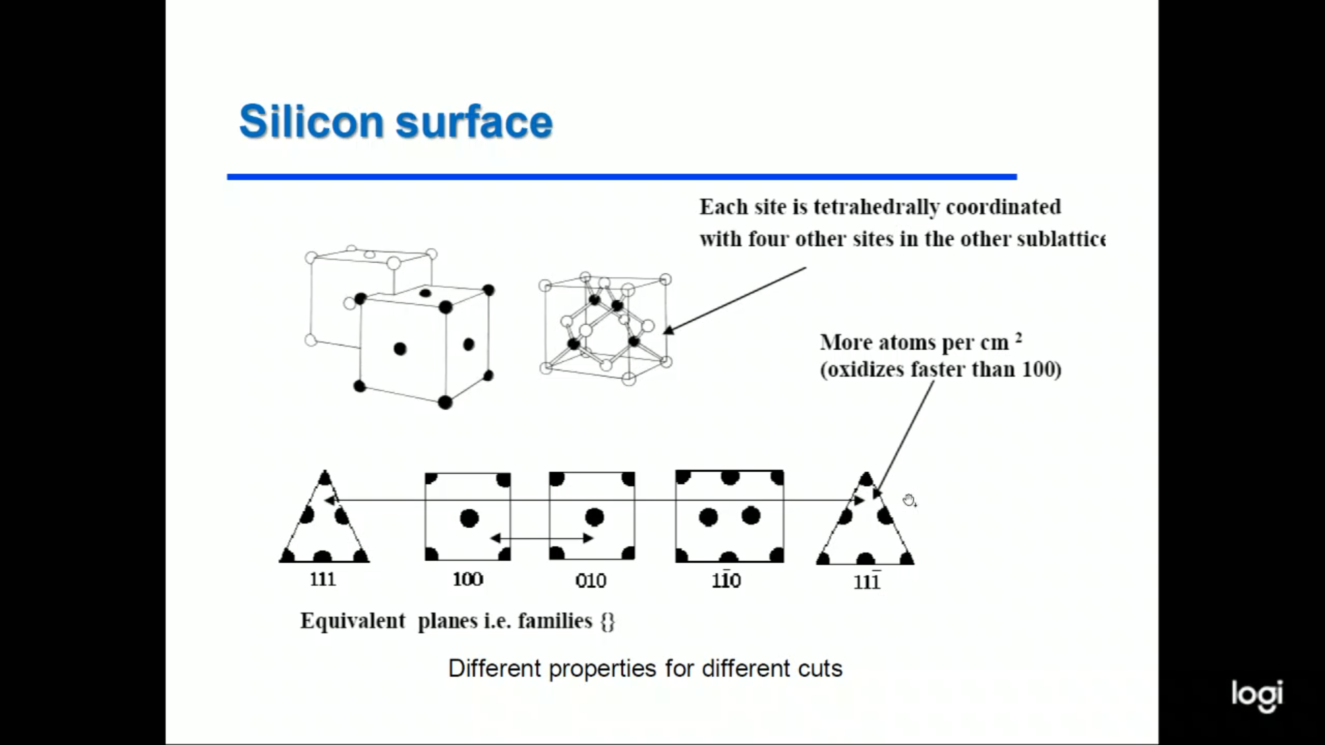
- Silicon
- IC Techonology
- IC - Silicon Substrate (Wafer)
- IC - Thin Film Deposition
- IC - Doping
- IC - Wet & Dry Etching
- IC - Photolithography
- IC - Evolution of the Density of Transistor
- MS (Two Technologies)
- MEMS - Surface Bulk Micromachining
- MEMS - Anisotropic Etching
- Comparison between Inosotropic and Anisotropic Etching
- IC - Etch-Stop
- Basic Structures for Bulk Micromachining
- Preassure Sensor
- Cantilever
- Accelerometer
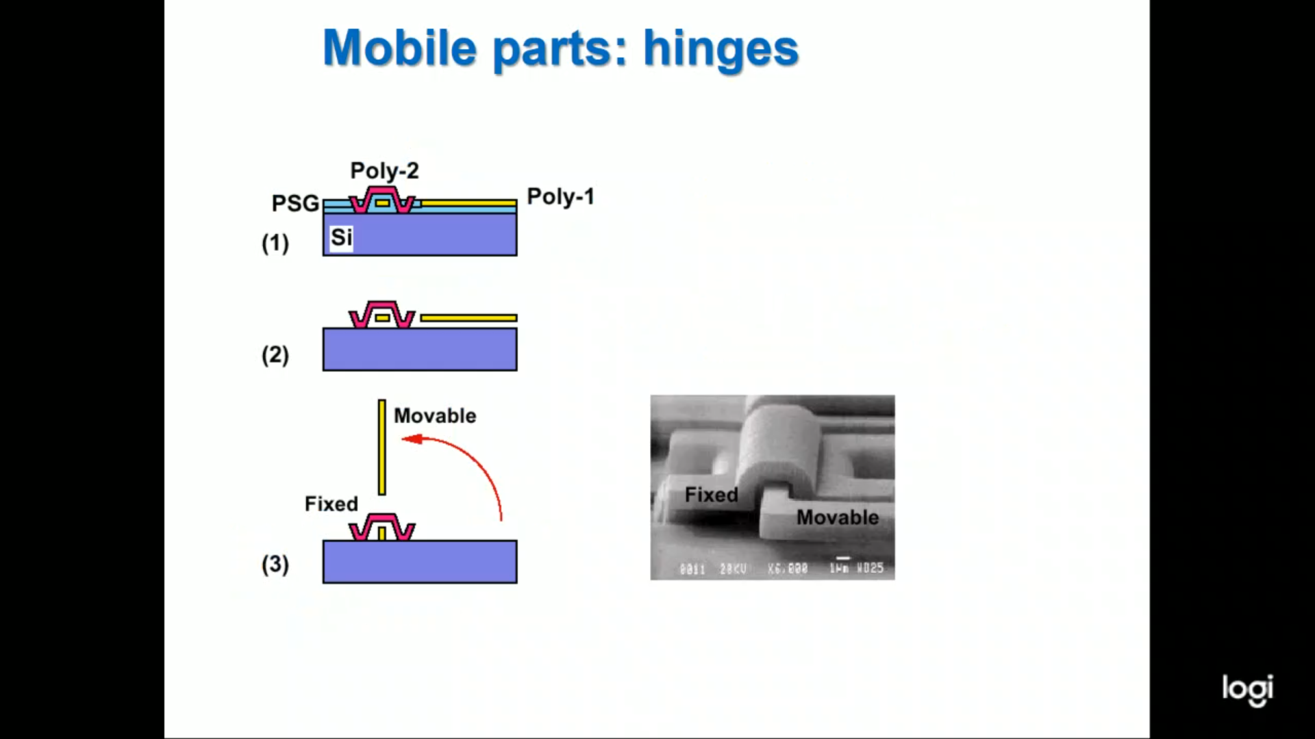
- Surface Micromachining
- Force Primary Sensor (Balance)
- Capacitive Accelerometer
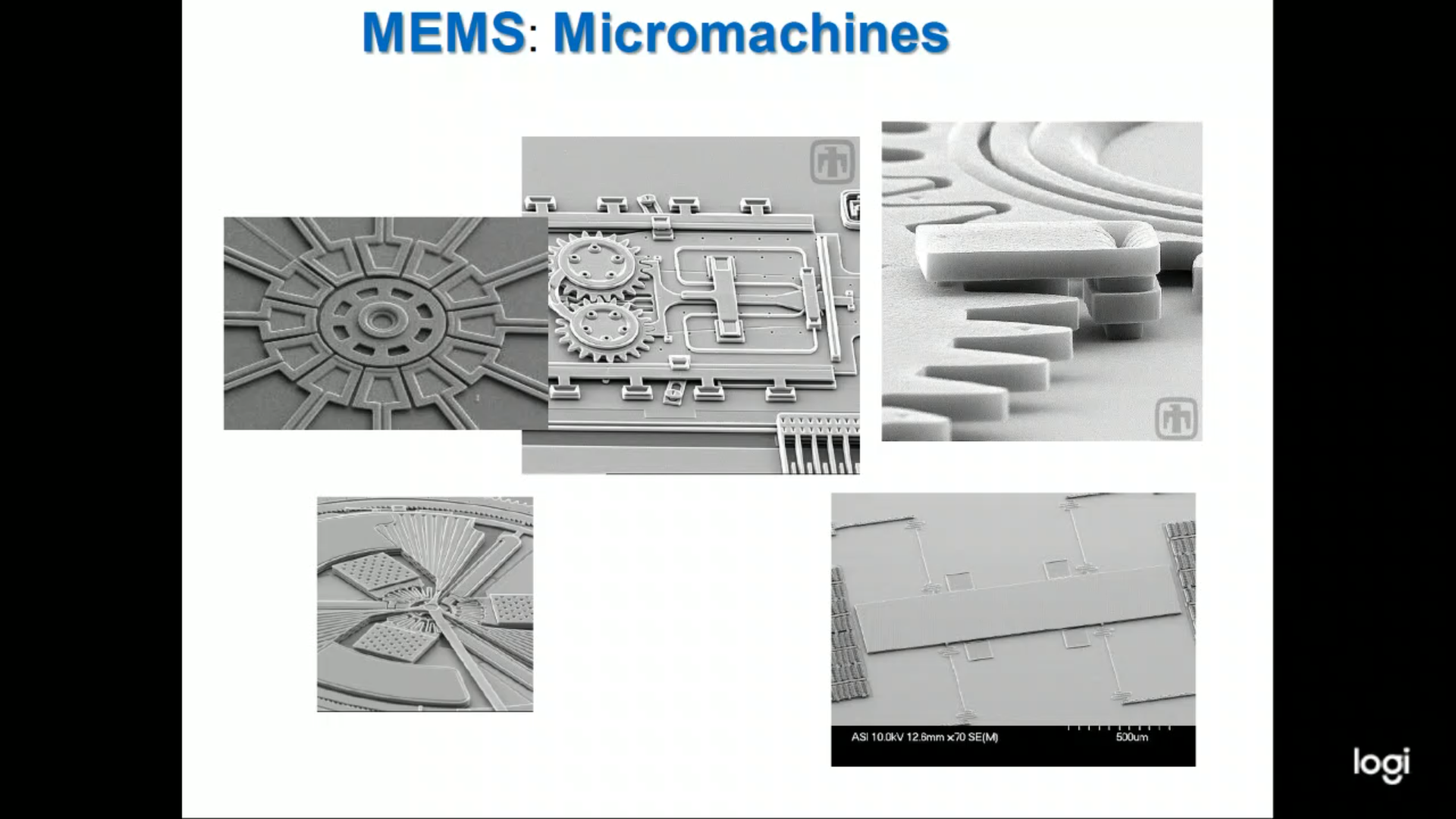
- Complex Micromachine
- MEMS - Accelerometer
- MEMS - Accelerometer Chip View
- MEMS - Gyroscope
- MEMS - Pressure Sensor (Lecture Recap)
- MEMS - Flow Sensor
- Microphone
- Where to Find Accelerometer (Real World Vendor Site)
MEMS - Introduction
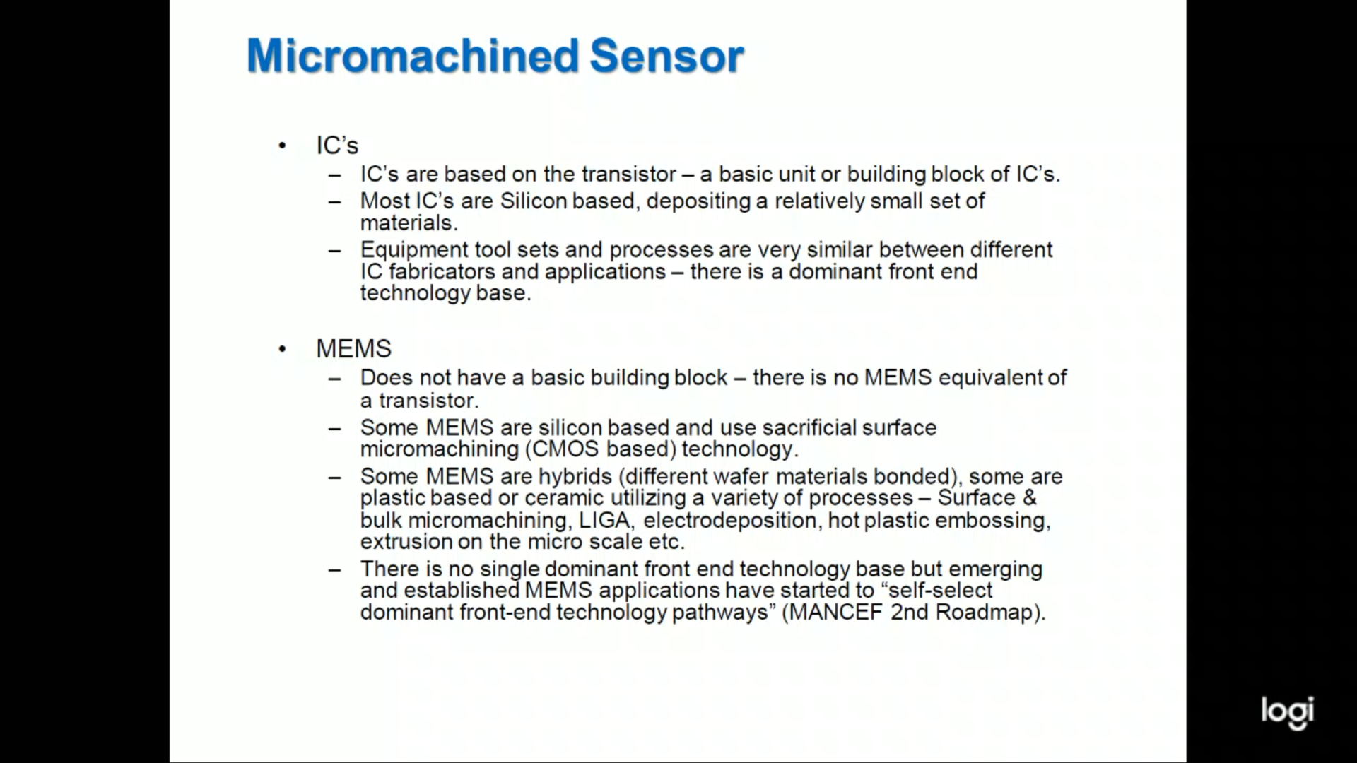
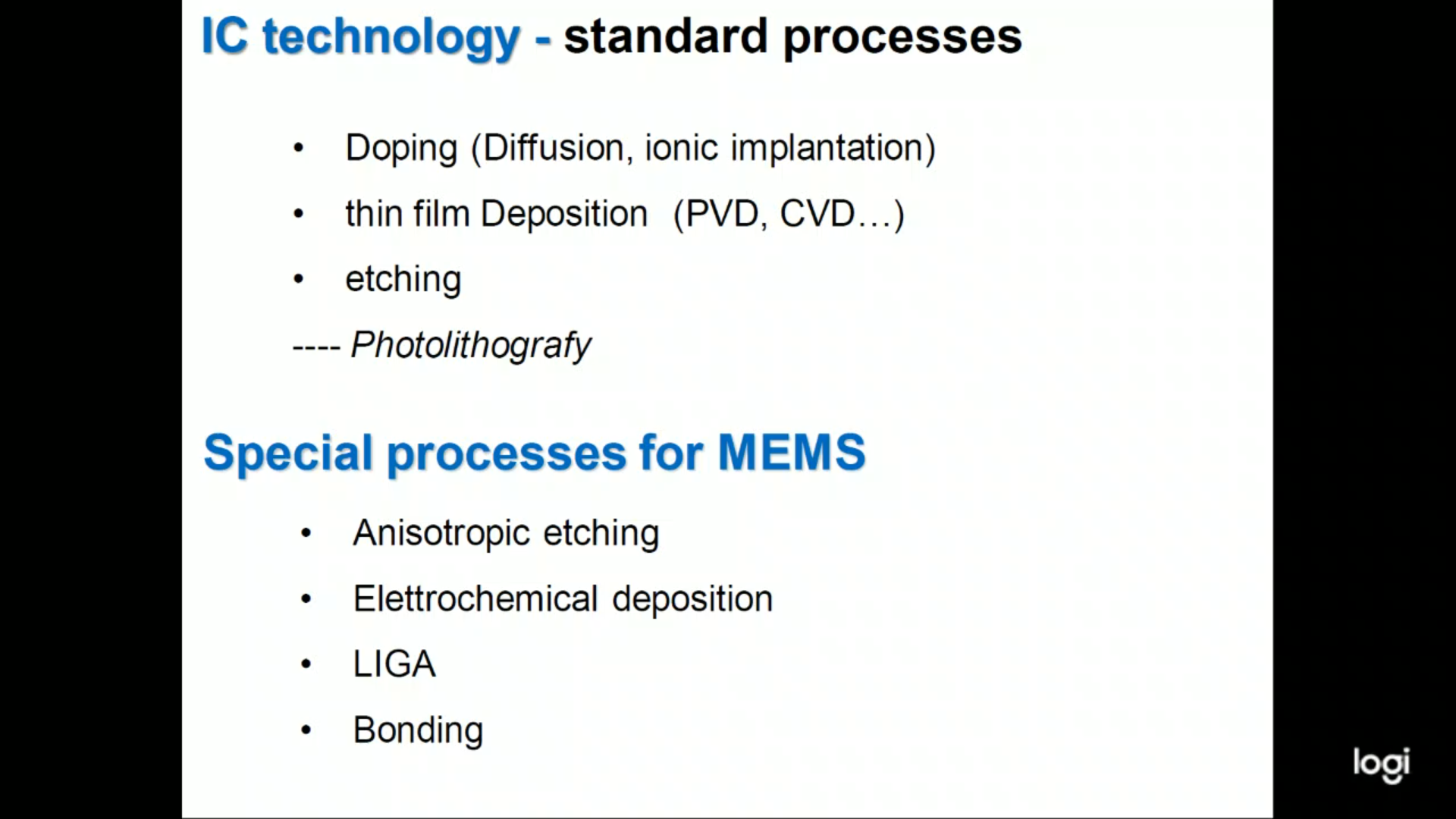
- ==The difference between IC technology and MEMS technology, is that MEMS derives some steps, but then add some steps which are not so standard as the IC technology==.
This is the most important thing. - ==So, MEMS are developed using the normal route which is used for IC, but then there are some special steps which are used==.
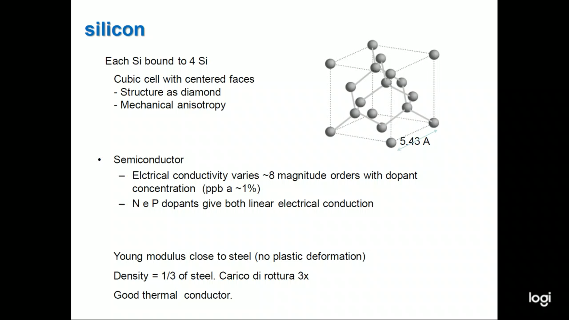
Silicon
IC Techonology
- What does LIGA means when we talk about special processes for MEMS creation?
- ==LIGA is an acronym that stands for Lithographie, Galvanoformung, and Abformung, which translates to Lithography, Electroplating, and Molding in English.
It refers to a specialized process used in the creation of microelectromechanical systems (MEMS)==. - The LIGA process is a combination of techniques that enables the fabrication of high-precision and high-aspect-ratio microstructures.
It is particularly suited for the production of microstructures with complex geometries and tight tolerances. - Here’s a brief overview of the three steps involved in the LIGA process:
- Lithography: The first step in the LIGA process is lithography, which involves the use of photolithographic techniques to pattern a photoresist material.
A photosensitive resist is deposited onto a substrate, and a mask or pattern is used to selectively expose and develop the resist, forming a precise pattern of the desired microstructure. - Electroplating: After lithography, the patterned resist serves as a mold or template for the electroplating process.
The substrate with the patterned resist is immersed in an electroplating bath containing the desired metal or material.
An electric current is applied, causing the metal ions in the bath to deposit onto the exposed areas of the substrate, growing the microstructure layer by layer.
This electroplating step allows for the creation of high-aspect-ratio structures. - Molding: The final step of the LIGA process is molding, where the electroplated microstructure is separated from the substrate.
The resist material is typically dissolved or removed, leaving behind the free-standing microstructure.
The molded microstructure can then be further processed, assembled, or integrated into MEMS devices.
- Lithography: The first step in the LIGA process is lithography, which involves the use of photolithographic techniques to pattern a photoresist material.
- The LIGA process offers several advantages for MEMS fabrication, including the ability to produce complex 3D structures with high precision, repeatability, and scalability.
The process is often used in applications that require intricate microstructures, such as microfluidics, micro-optics, and microsensors. - It’s worth noting that LIGA is just one of the many specialized processes used in MEMS fabrication.
Other techniques, such as surface micromachining, bulk micromachining, and silicon-on-insulator (SOI) technology, are also employed depending on the specific requirements of the MEMS device being manufactured.
- ==LIGA is an acronym that stands for Lithographie, Galvanoformung, and Abformung, which translates to Lithography, Electroplating, and Molding in English.
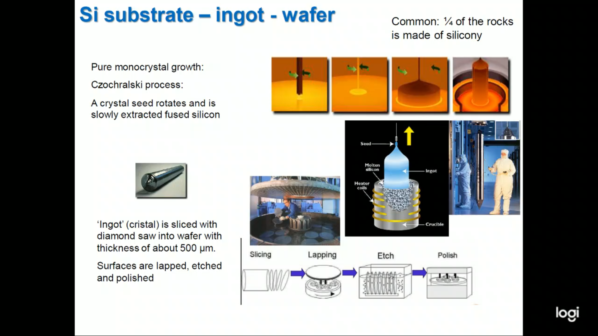
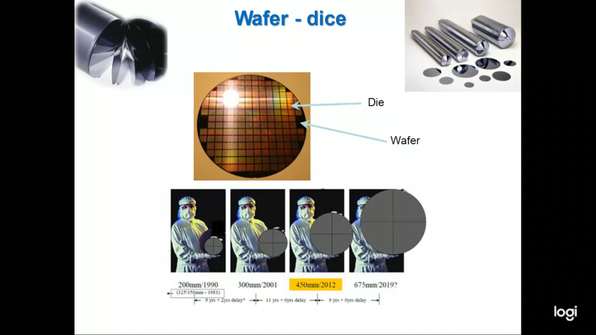
IC - Silicon Substrate (Wafer)
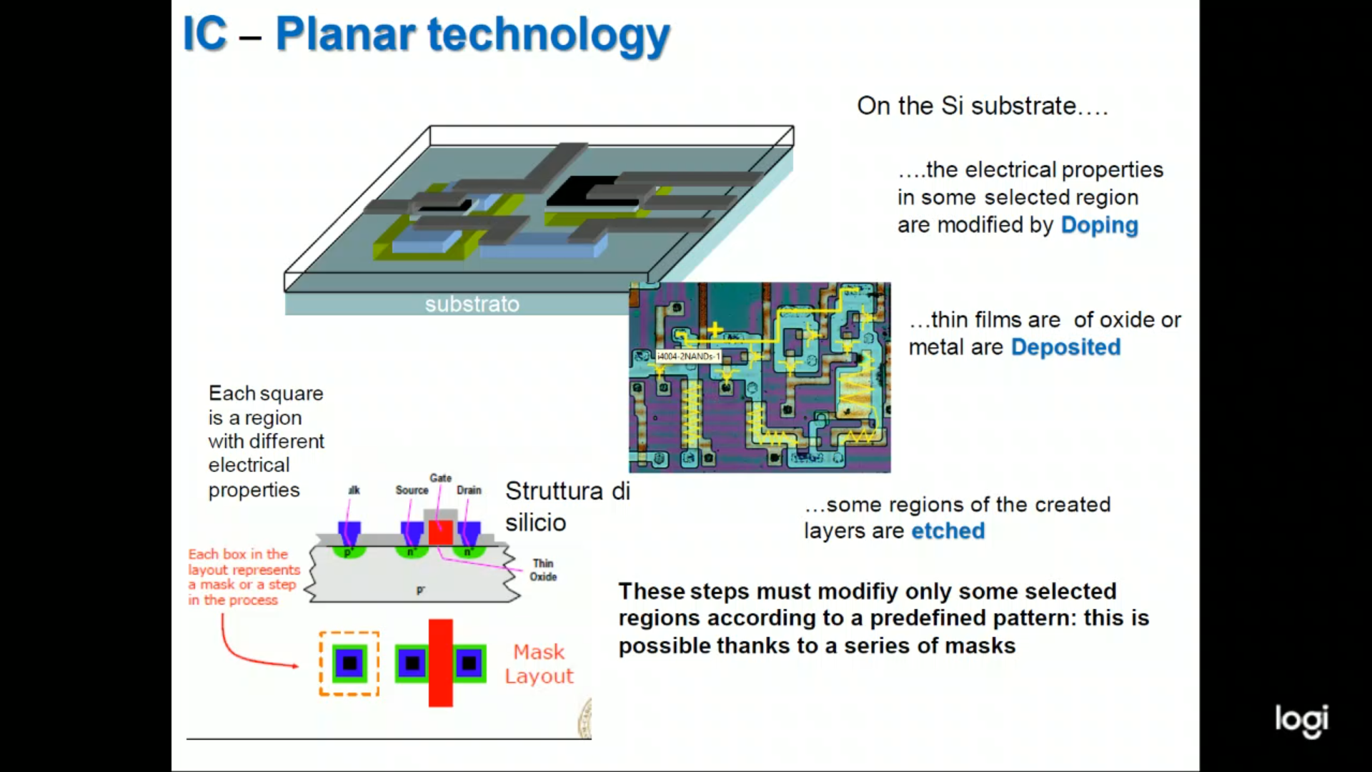
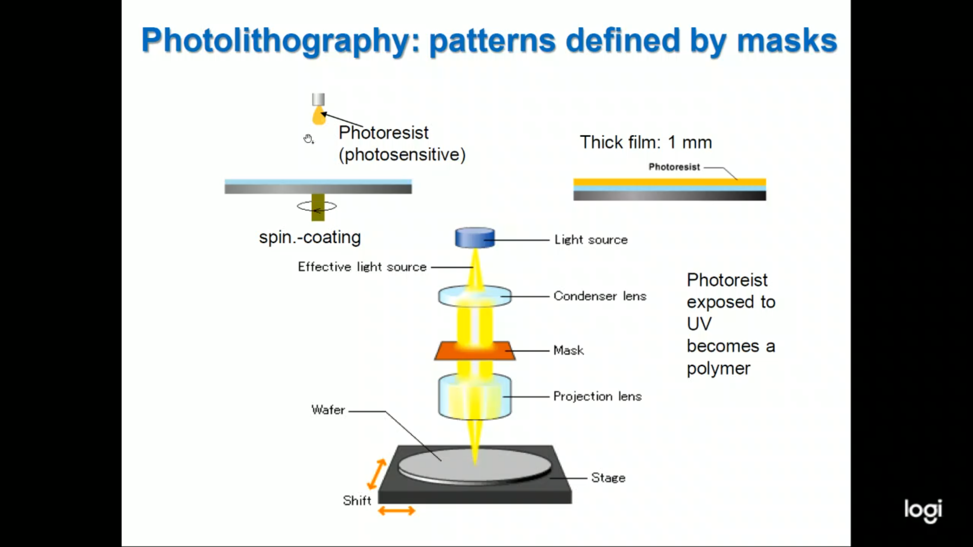
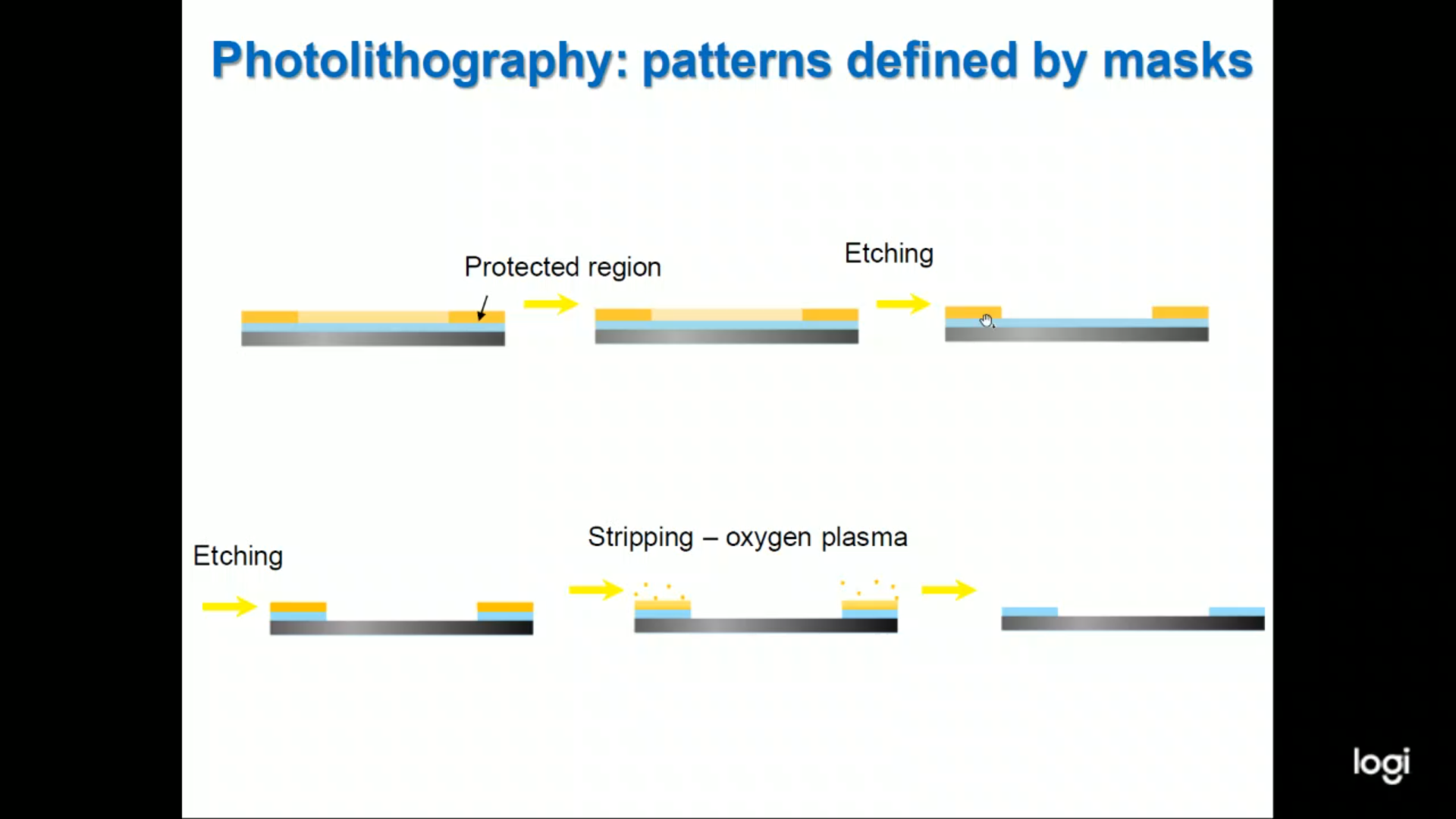
- ==Masks protect the wafer with the exception of the single region that has to be modified==.
- ==So when we design a chip, we actually desing different masks one for each step which can be doping, depositing or removing the film==.
ICs are integrated circuit which are developed with the planar technology. So it is all obtained on top of a substrate, a substrate which is a pure silicon slice, also called wafer. Some regions of the slice of the wafer are modified from a point of view of electrical properties by doping. And we know that by creating a doped region we may have resistors, diodes and transistors. And then there is a deposition of the wires and the connection between the different devices which are created with doping, and these are obtained by deposition of metal.
And since we need many, many metal wires, then we need also to insulate some regions in order to avoid electrical contact, and so also oxide films are deposited. And obviously the process that it is used in order to create different regions with different properties needs also to remove some layers of material, and this is done by a process which is called etching. So placing films and etching some part of the films. So depositing and etching at the end we can get the overall structure of the circuit.
And here you can see for instance a cross section of a MOSFET: So two doped regions are needed for drain and source, then ther is a thin layer of oxide below the gate. And then there are these metal lines here which are drain, gate and source contact. Instead the drain layer is an insulator. So this placement of different regions is done through the design of masks.
IC - Thin Film Deposition
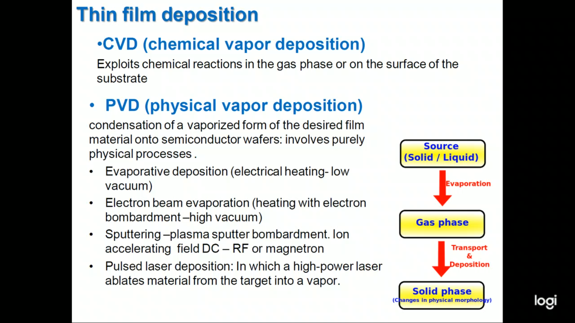
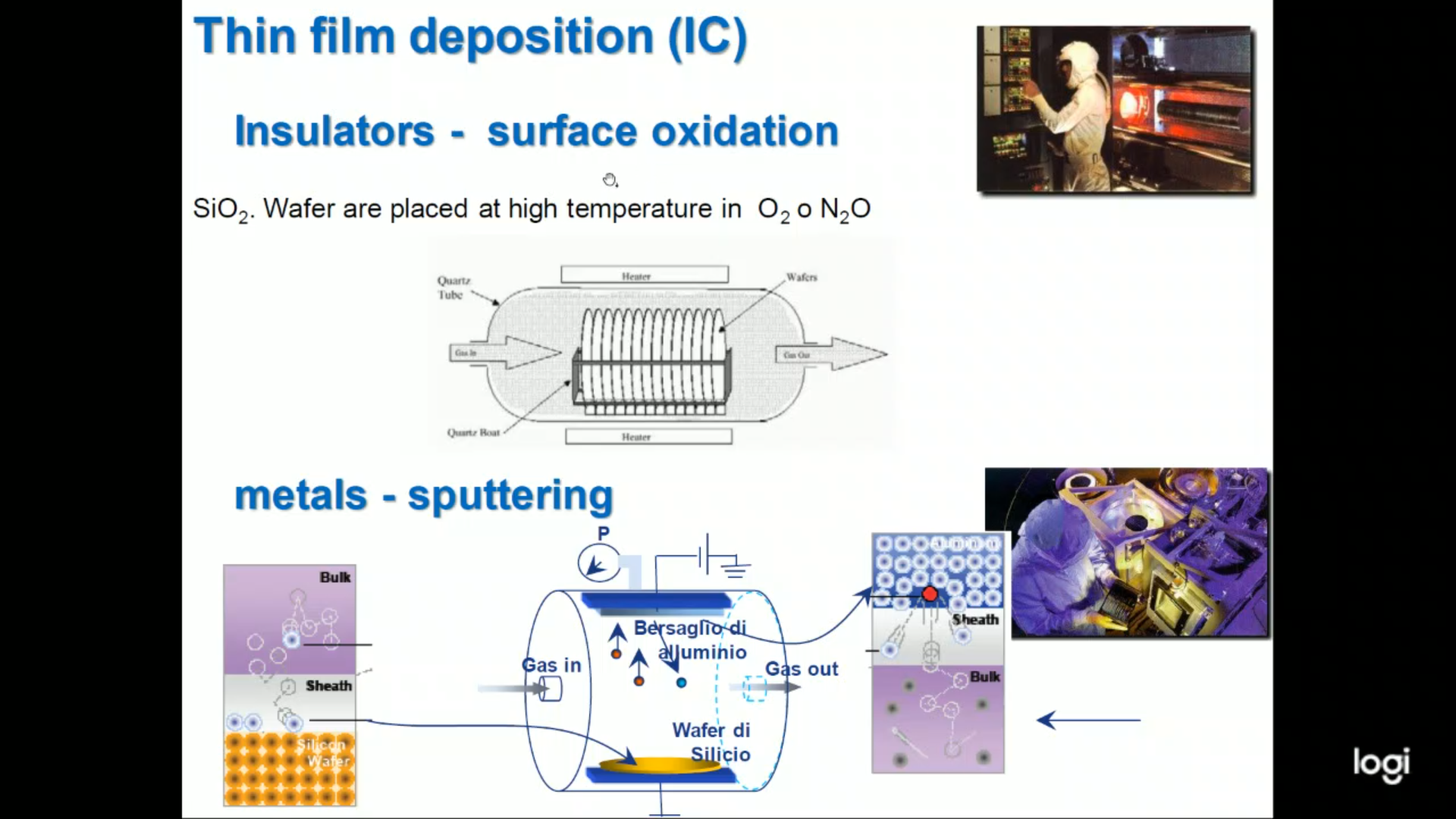
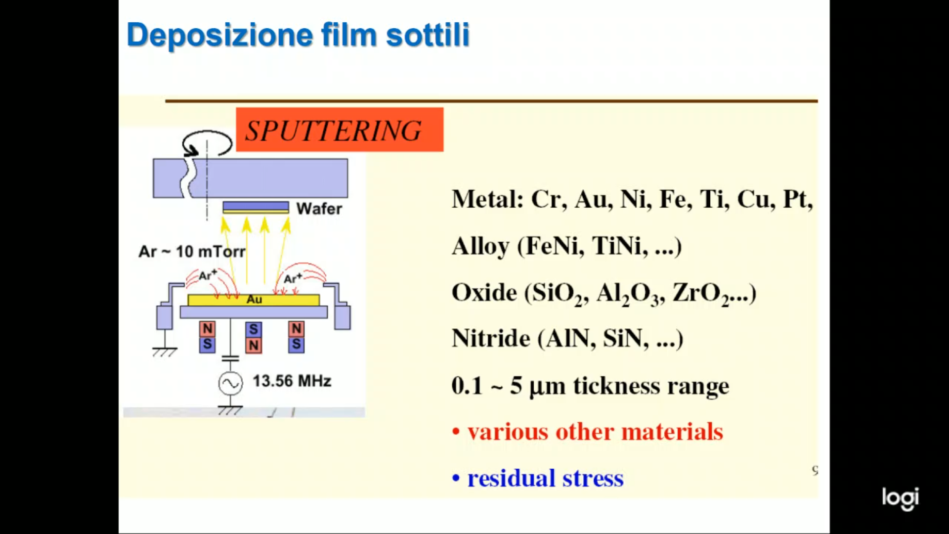
- ==So by heating this target with ions, some of the metal atoms are extracted from the film, and then they are deposited on the silicone wafer, and with this you can create very, very thin metal layers==.
IC - Doping
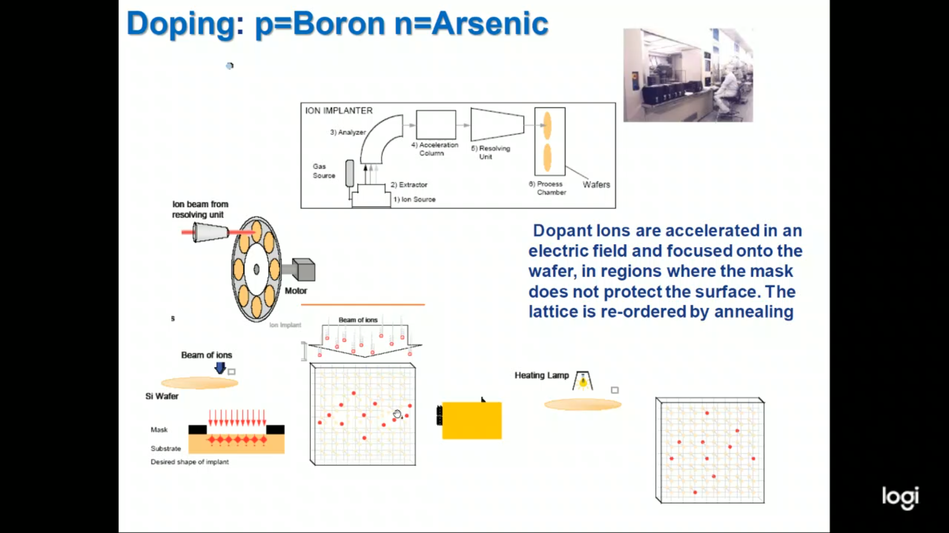 ==Here we see the ion implantation that is that the impurities, the dopants, are placed in the silicone lattice by means of “impinging” accelerated ions.
So for instance, phosphor or others are accelerated by an electrical field, and then they hit the silicone substrate, therefore they penetrate the lattice, and then after this process, the second process of annealing which is hitting, allows to the lattice to get back to a good order and you obtain in this way a doped material, as we can see in this figure here.
Mask protects the part you don't want to dope.
So for this reason this is better than the fusion doping==.
==Here we see the ion implantation that is that the impurities, the dopants, are placed in the silicone lattice by means of “impinging” accelerated ions.
So for instance, phosphor or others are accelerated by an electrical field, and then they hit the silicone substrate, therefore they penetrate the lattice, and then after this process, the second process of annealing which is hitting, allows to the lattice to get back to a good order and you obtain in this way a doped material, as we can see in this figure here.
Mask protects the part you don't want to dope.
So for this reason this is better than the fusion doping==.
IC - Wet & Dry Etching
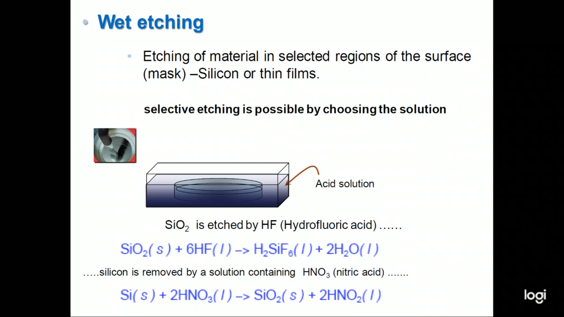
- ==This is wet etching because it’s done by chemical reaction in liquid phase==.
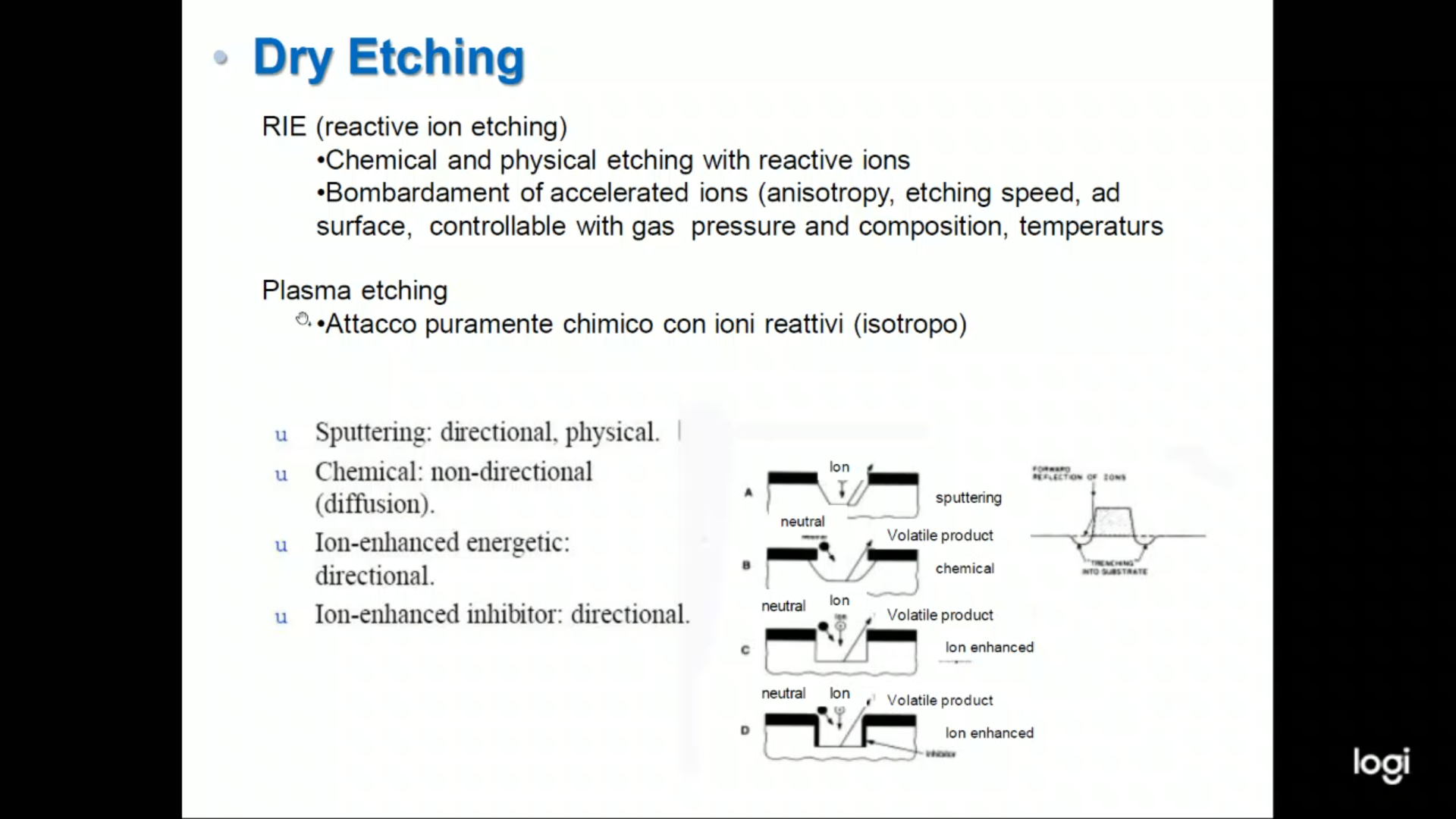
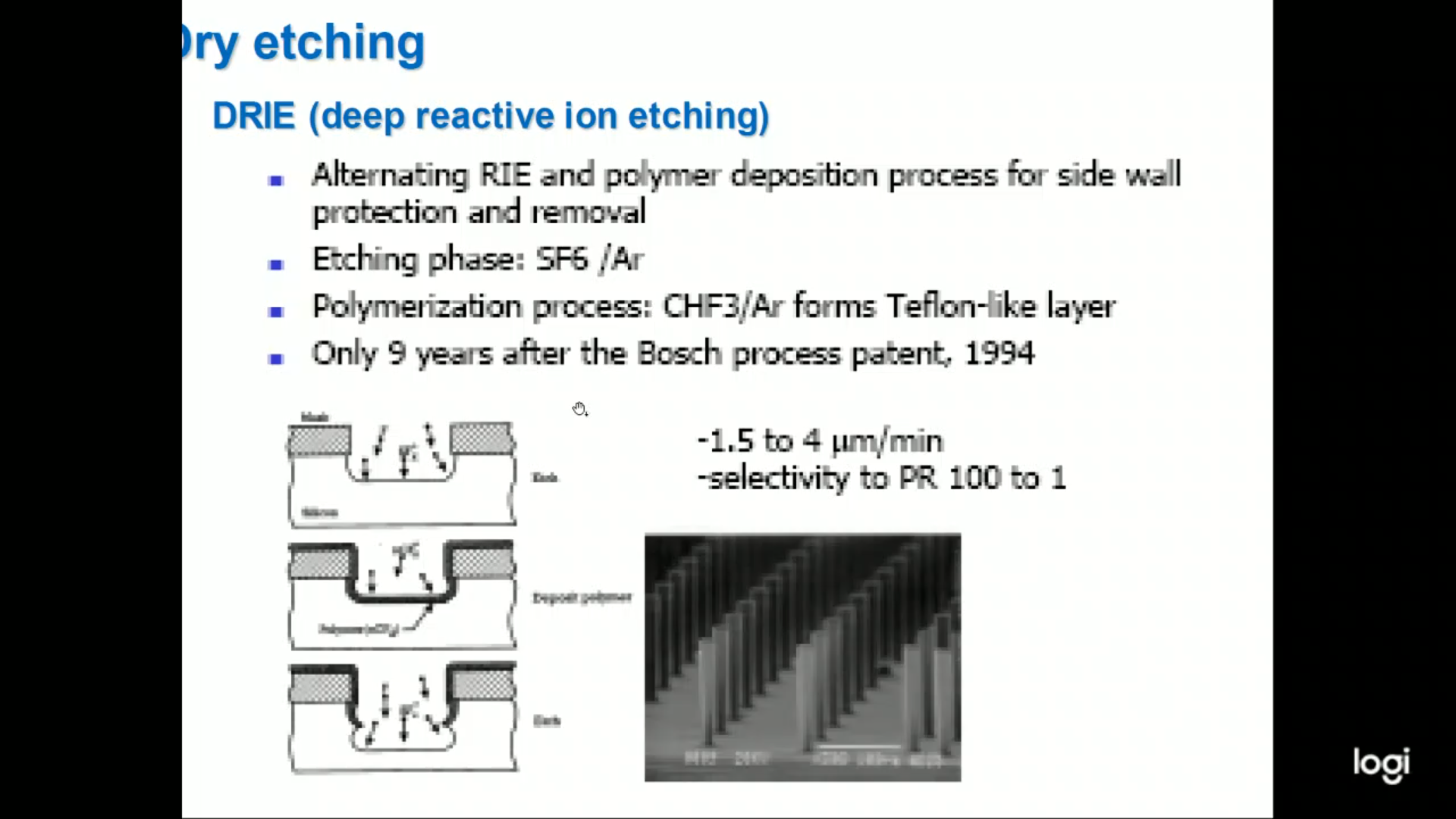
- ==Actually there is the possibility, also to remove something, by reactive ions which is a bombardment of oxidative ions, dry etching.
So the two possibilities, this is for sure more expensive, but more precise==.
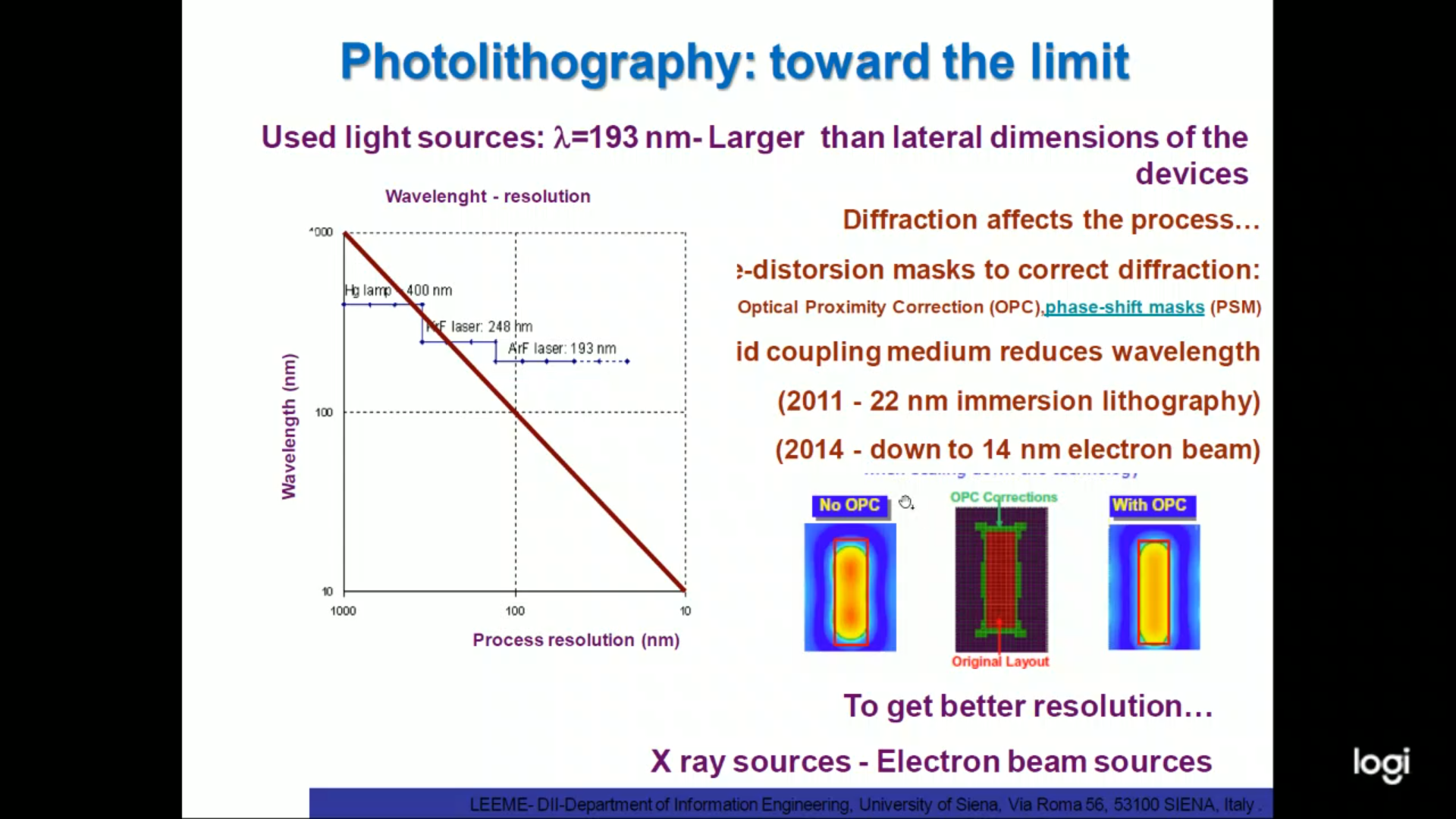
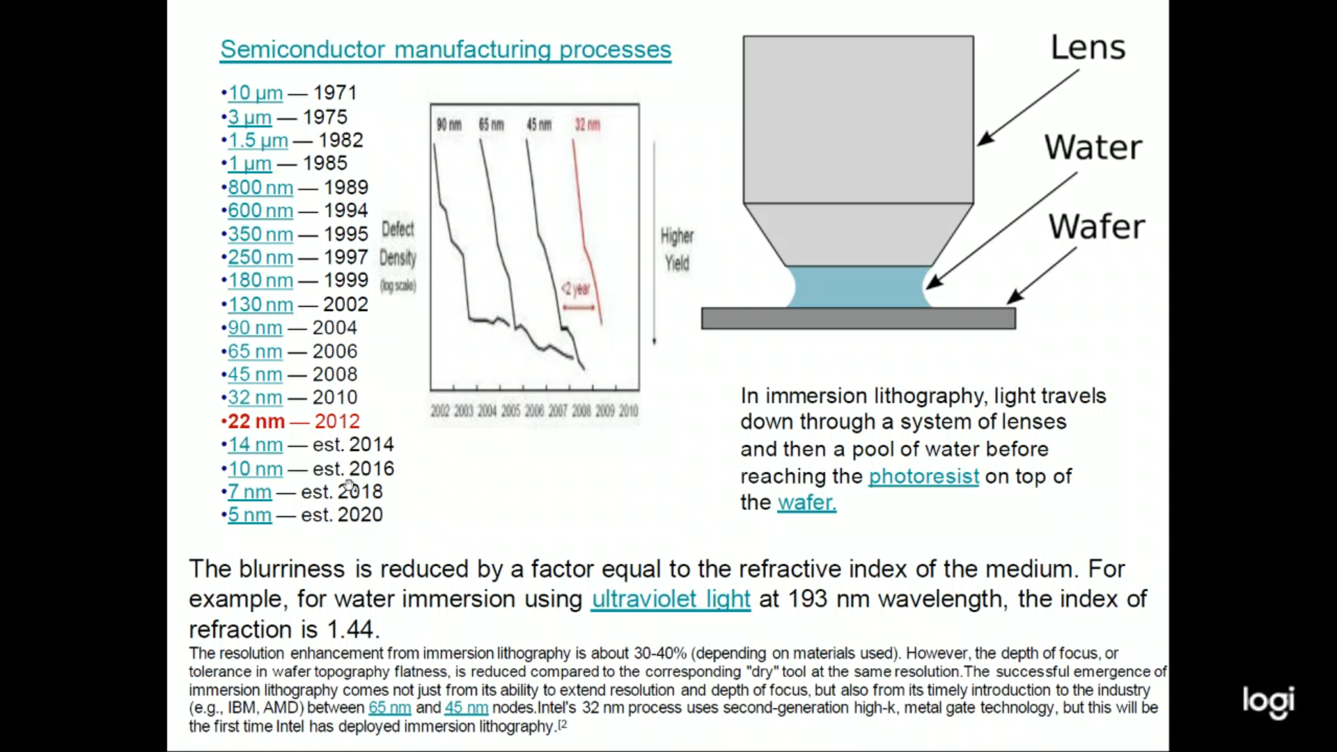
IC - Photolithography
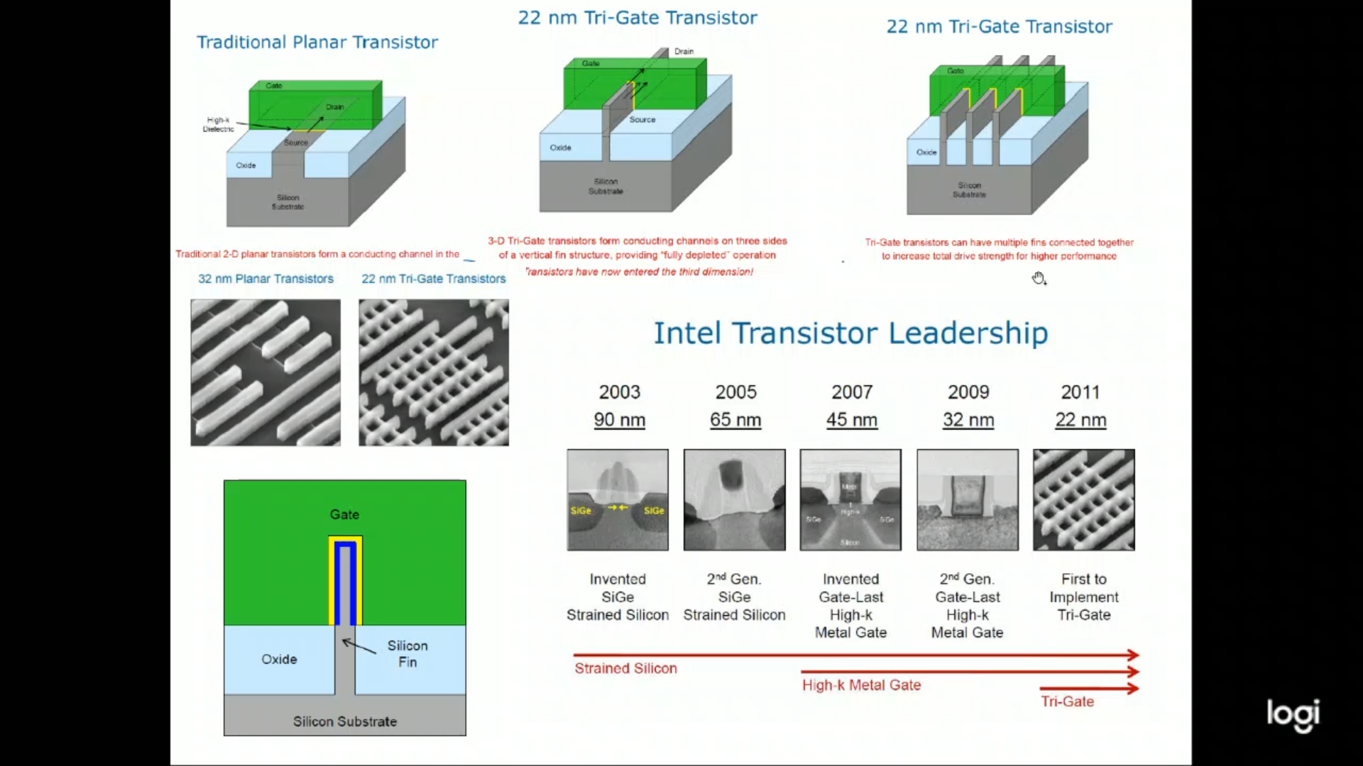
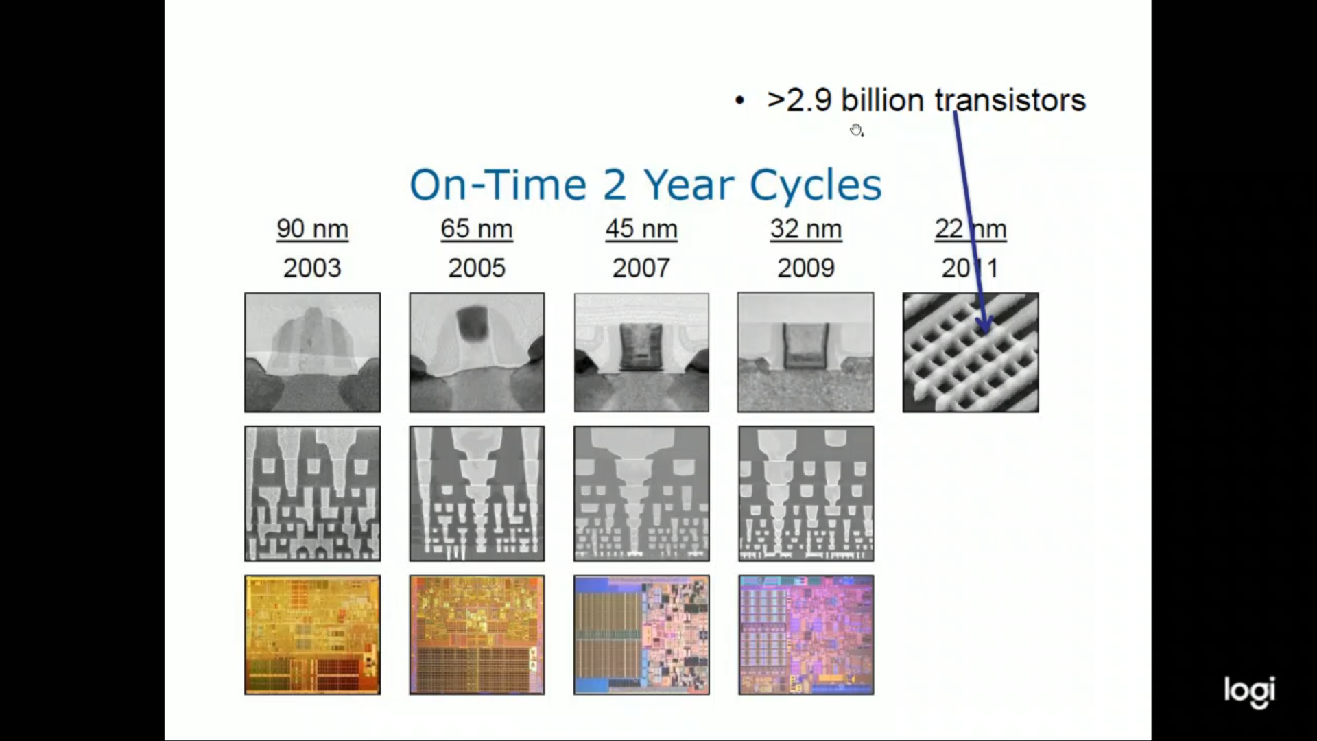
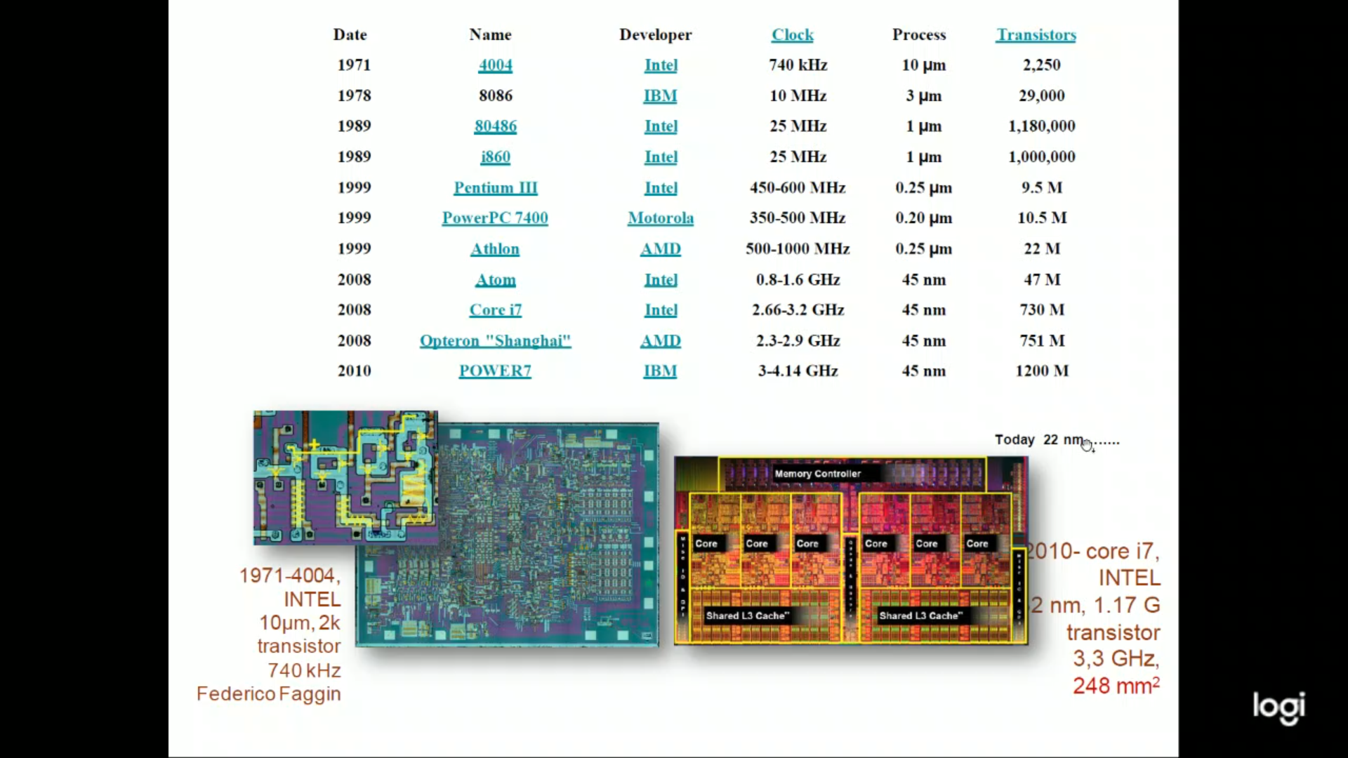
IC - Evolution of the Density of Transistor
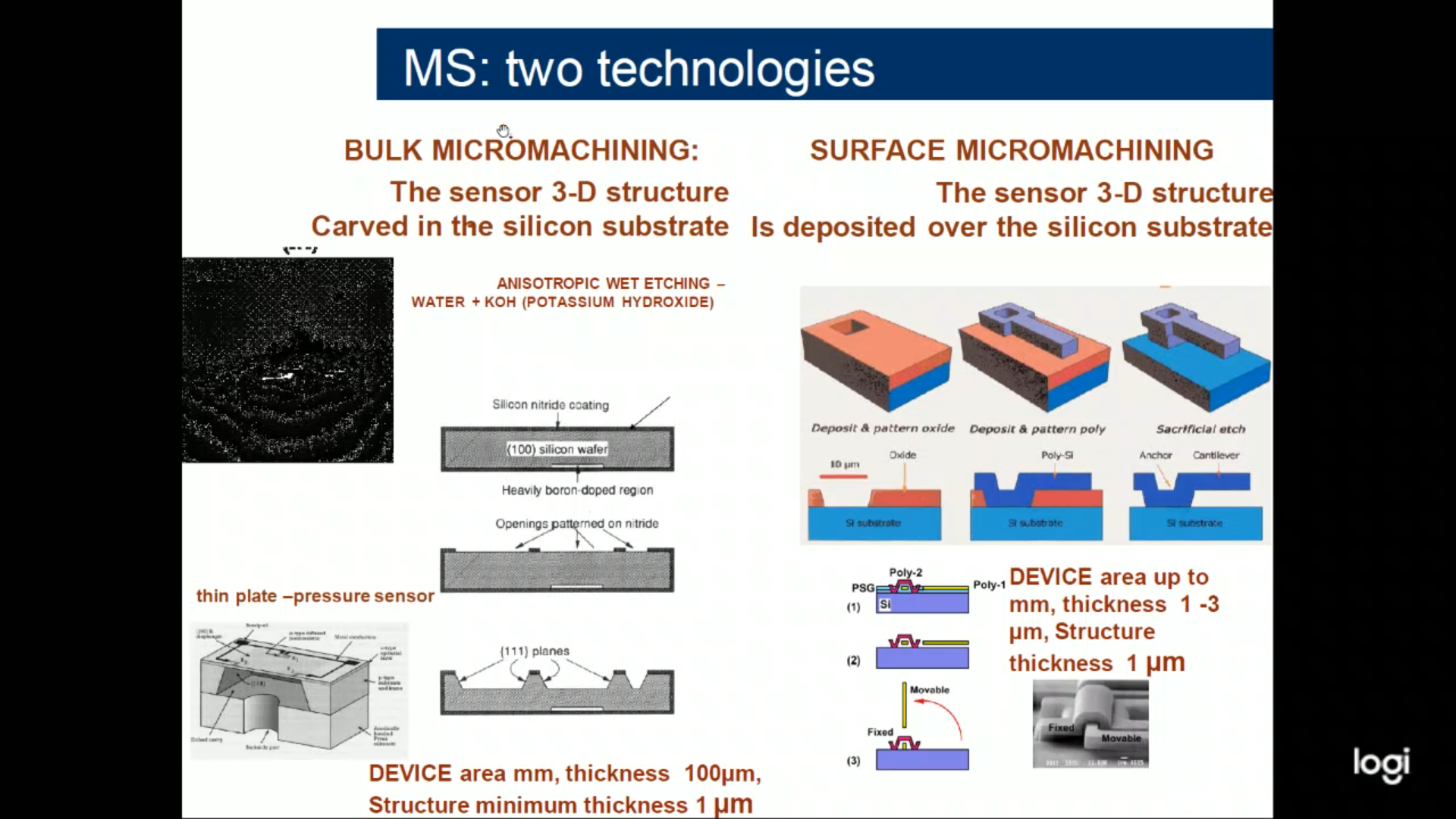
MS (Two Technologies)
 First of all:
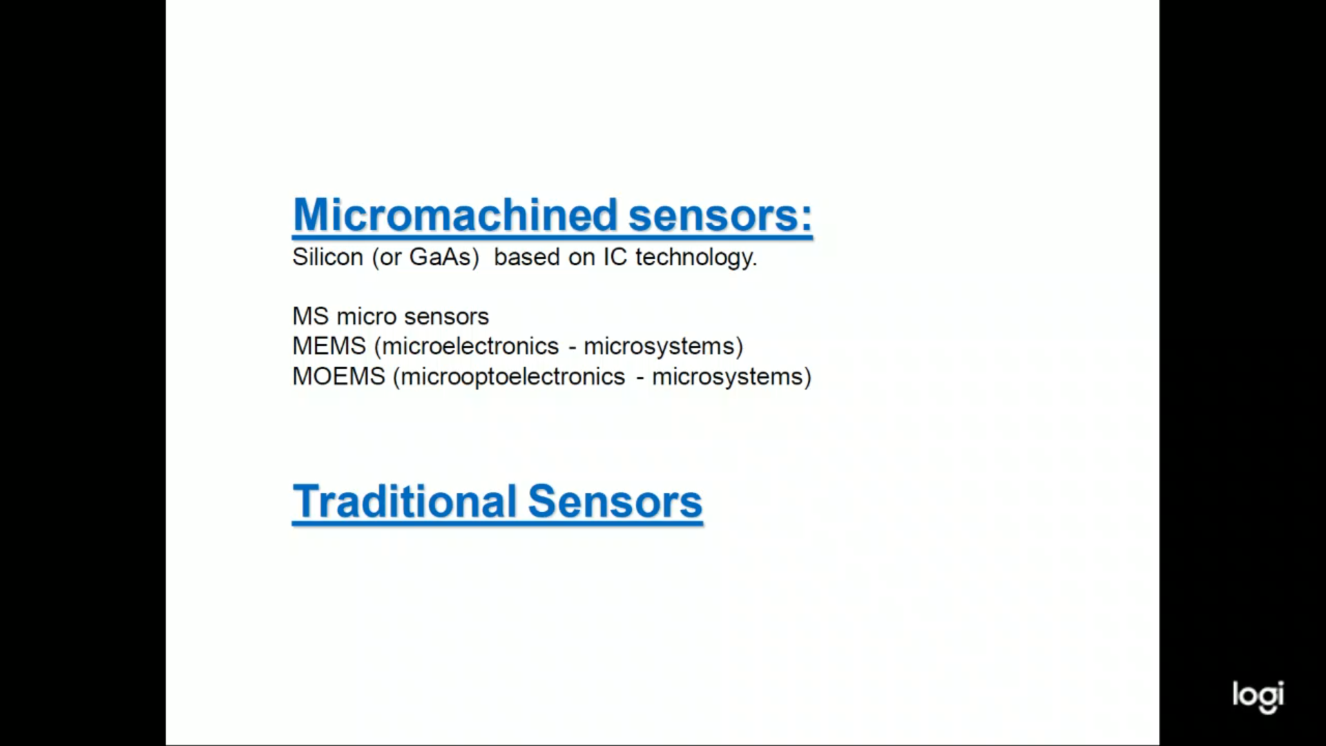
- MEMS means micro electro mechanical system.
- MS is micro sensor so something which is more general, let’s say.
MEMS - Surface Bulk Micromachining
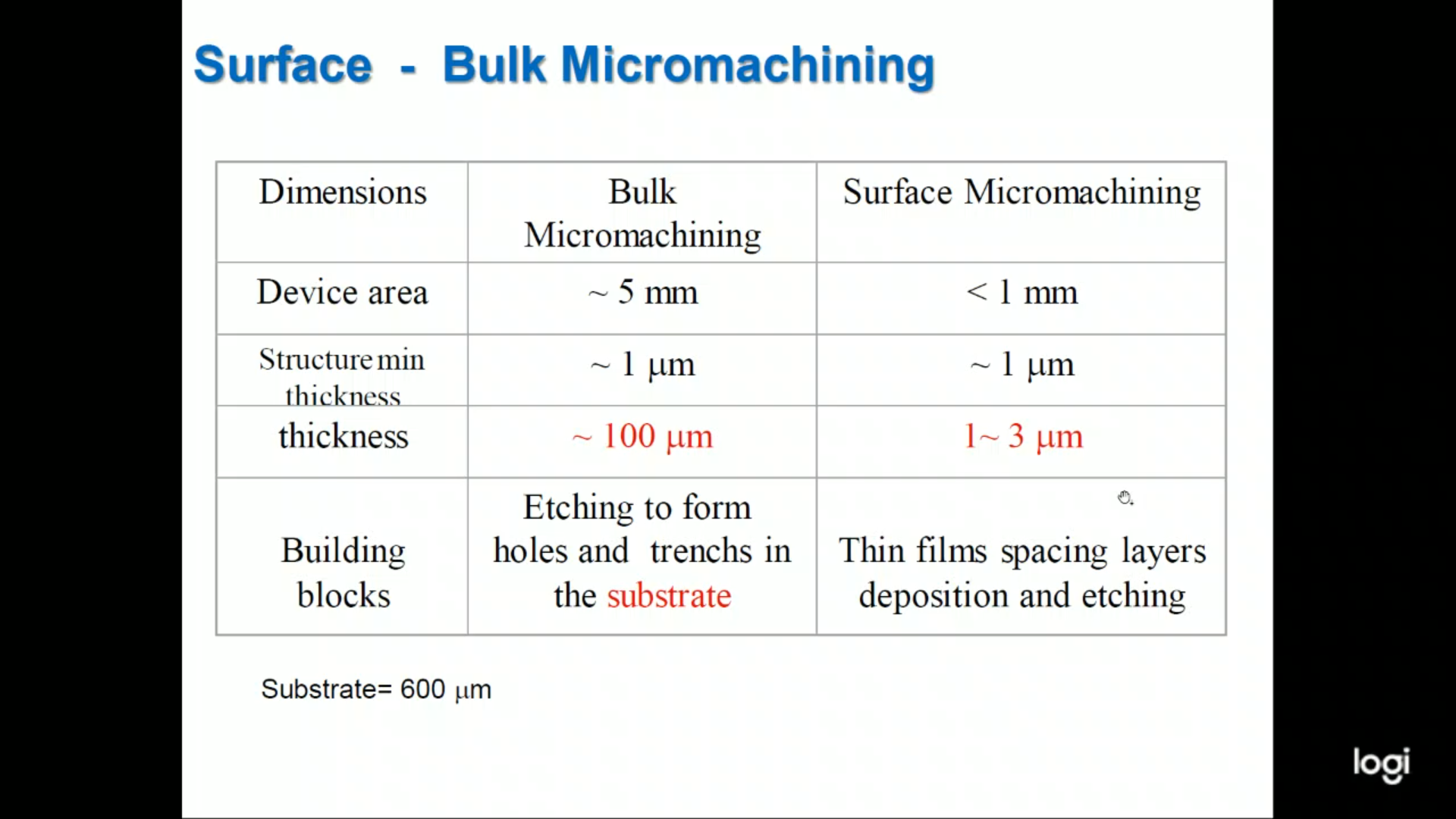
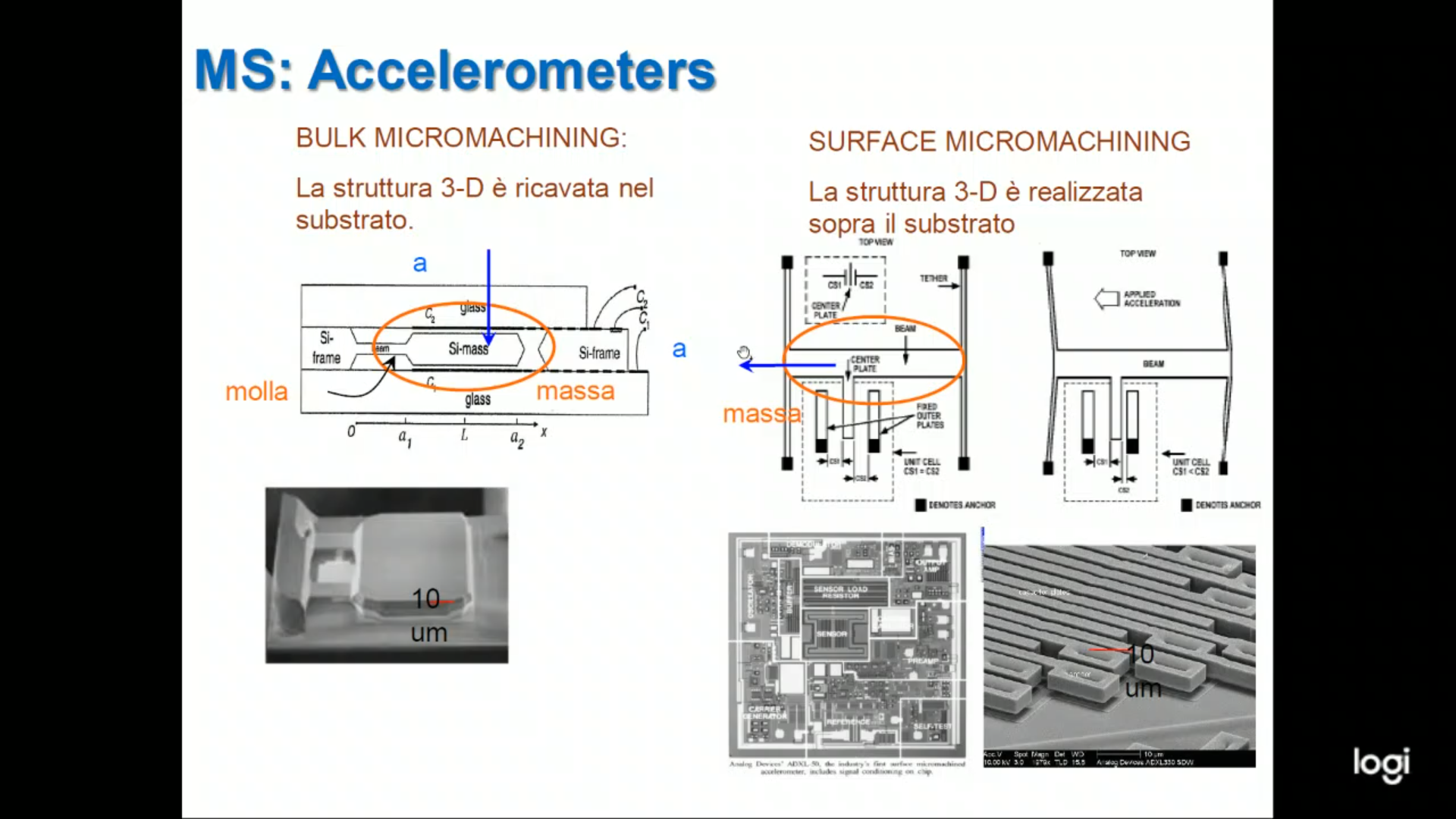
- ==Bulk micromachining, the sensor’s 3D structure is cut in the silicone substrate==.
- ==Surface micromachining allows to build a 3D structure over the substrate==.
So the wafer becomes a substrate, a backing, where on top of it the 3D structure is created.
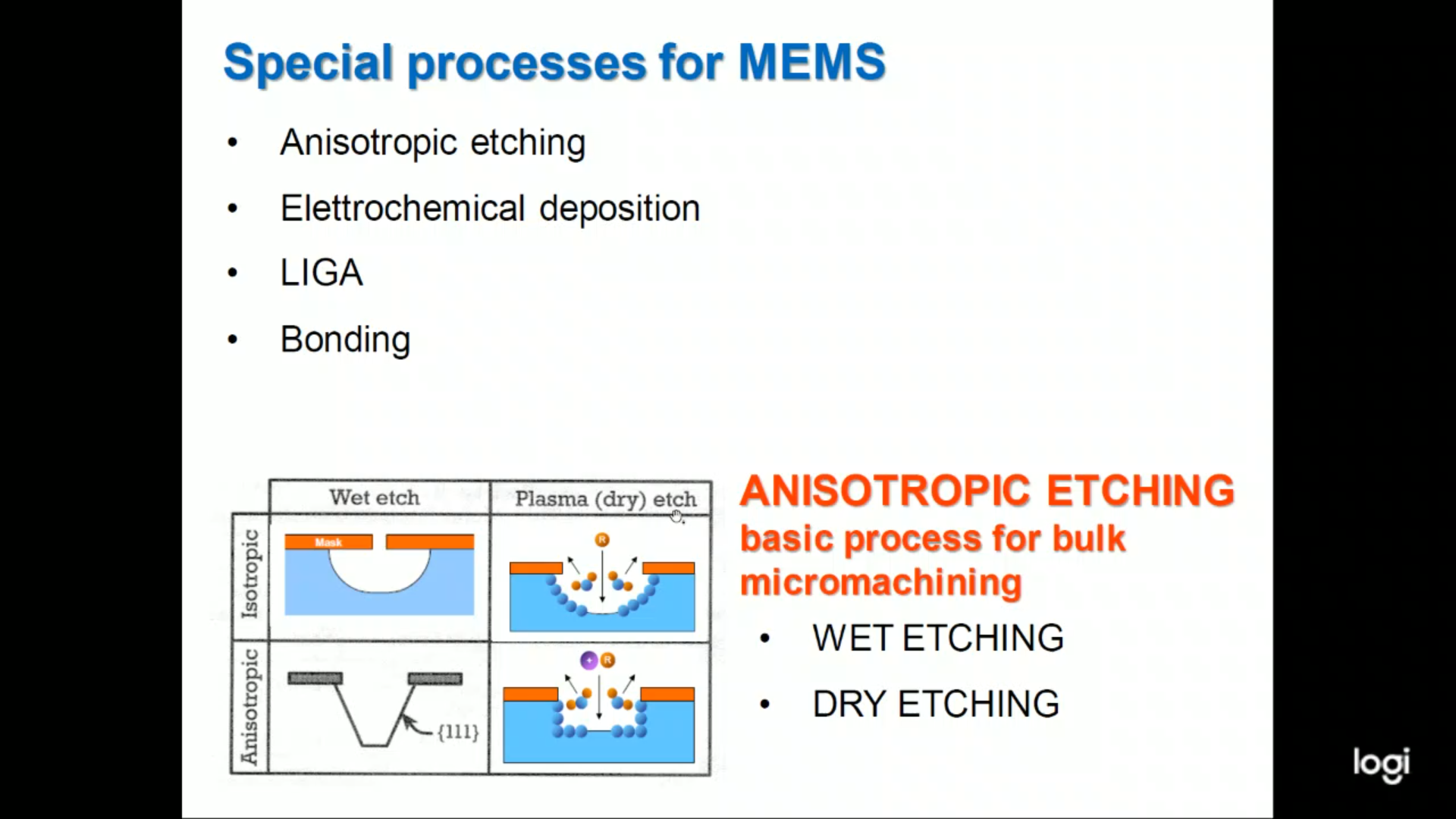
MEMS - Anisotropic Etching
- We have two types of anisotropic etching which is wet etching and dry etching:
- Dry etching is obtained with bombardment of ions, so plasma, which removes the silicone from some selected area, and the area are selected by masking as usual.
- Wet etching, the same idea, remove the silicone using instead a solution with an etching compound.
Comparison between Inosotropic and Anisotropic Etching
But what we see here is the comparison between anisotropic etching, dry or wet, and isotropic etching, wet or dry.
- You see that in anisotropic etching, there is a control of the side wall geometry.
- Instead with isotropic, it’s like having a sphere, so there is no control of the geometry of the side wall of the carving.
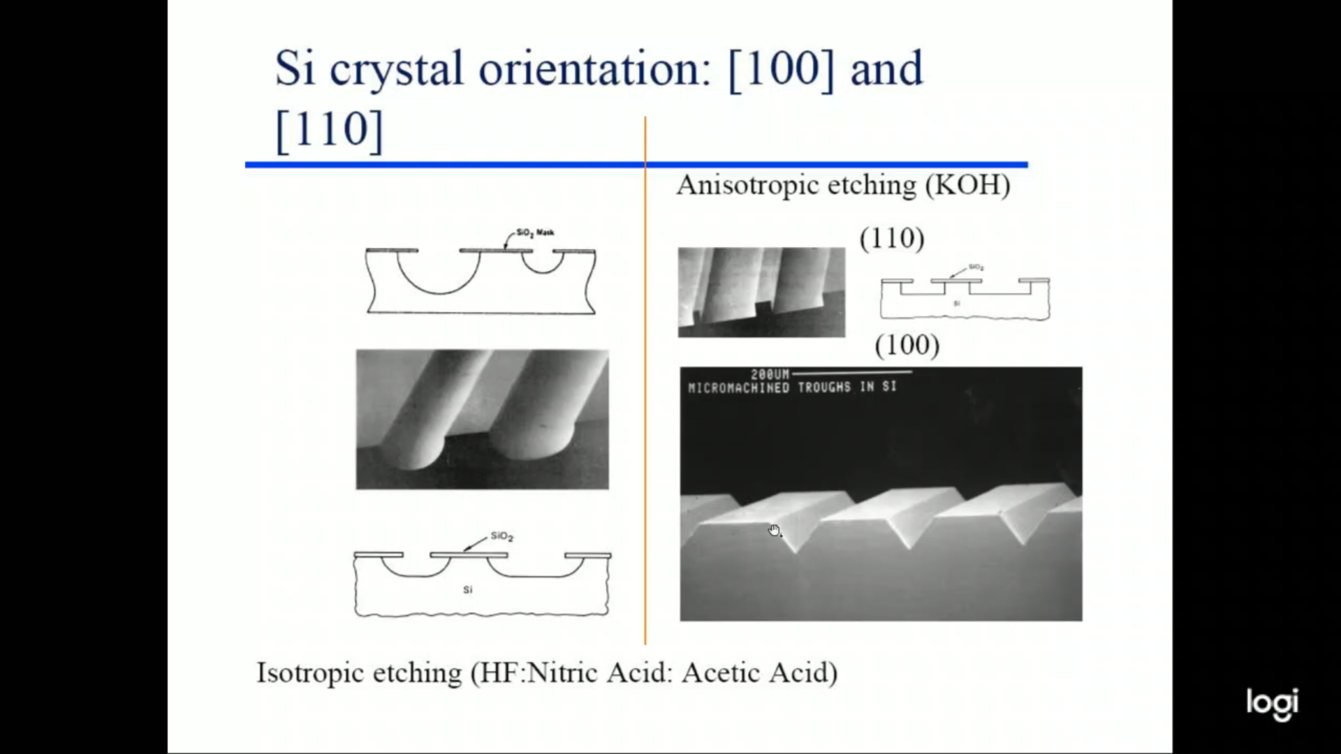
- Here you can see the clear difference between the two.
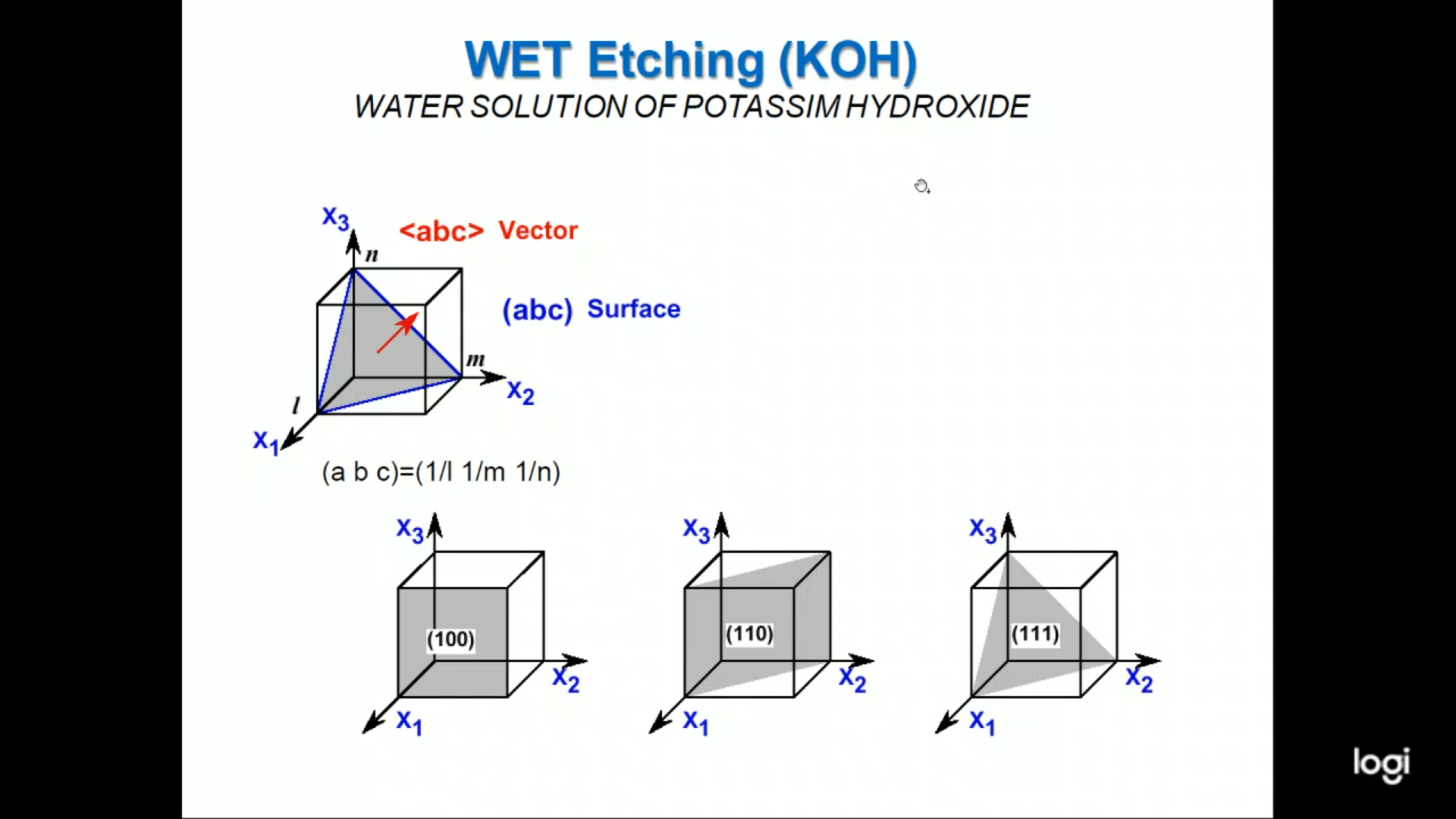
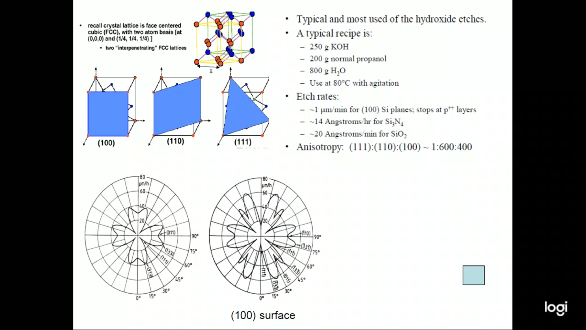
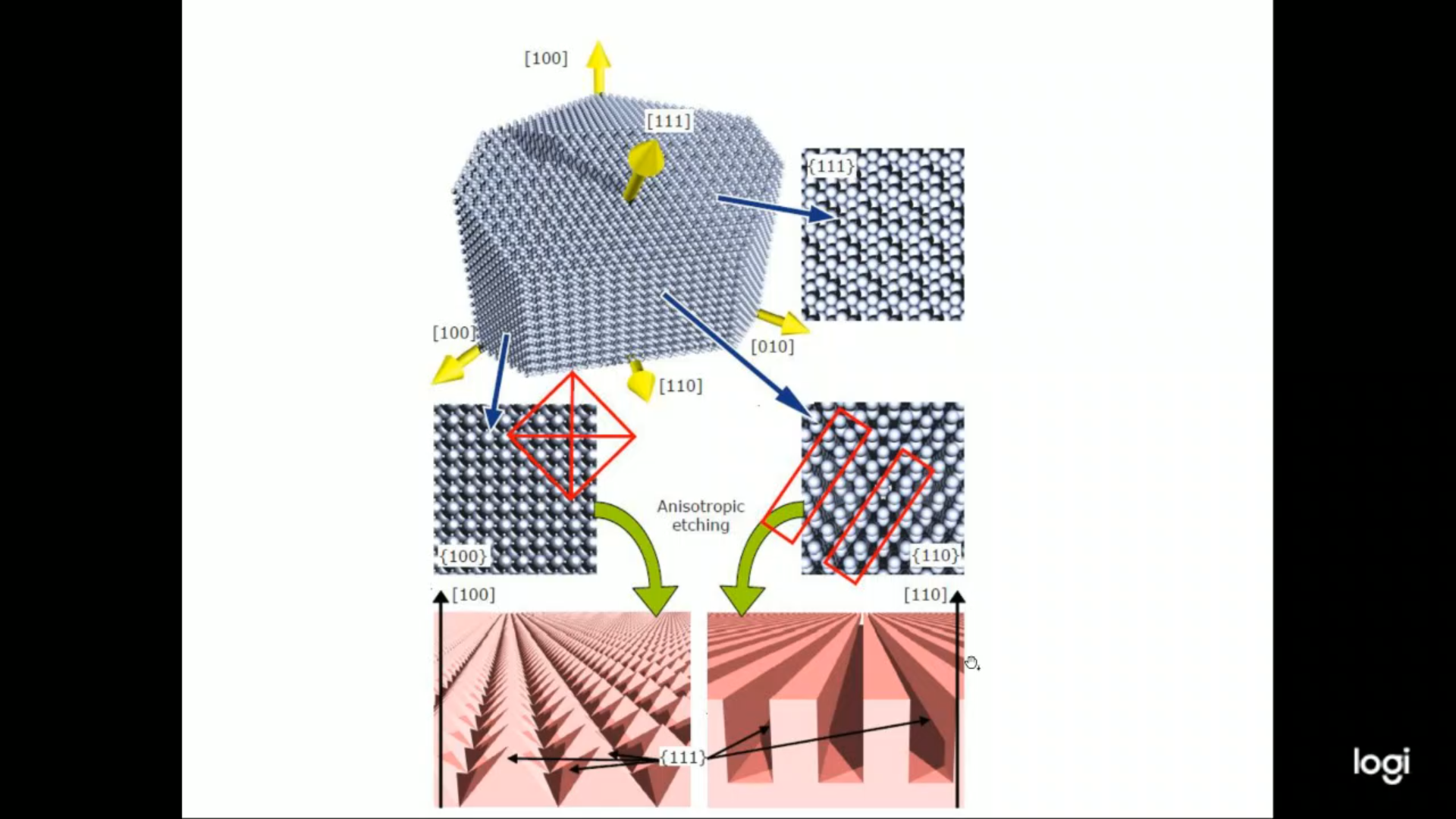
- Wet etching which was the first process used to obtain micromachine sensor, is an etching process based on special chemical agents, which is potassium hydroxide.
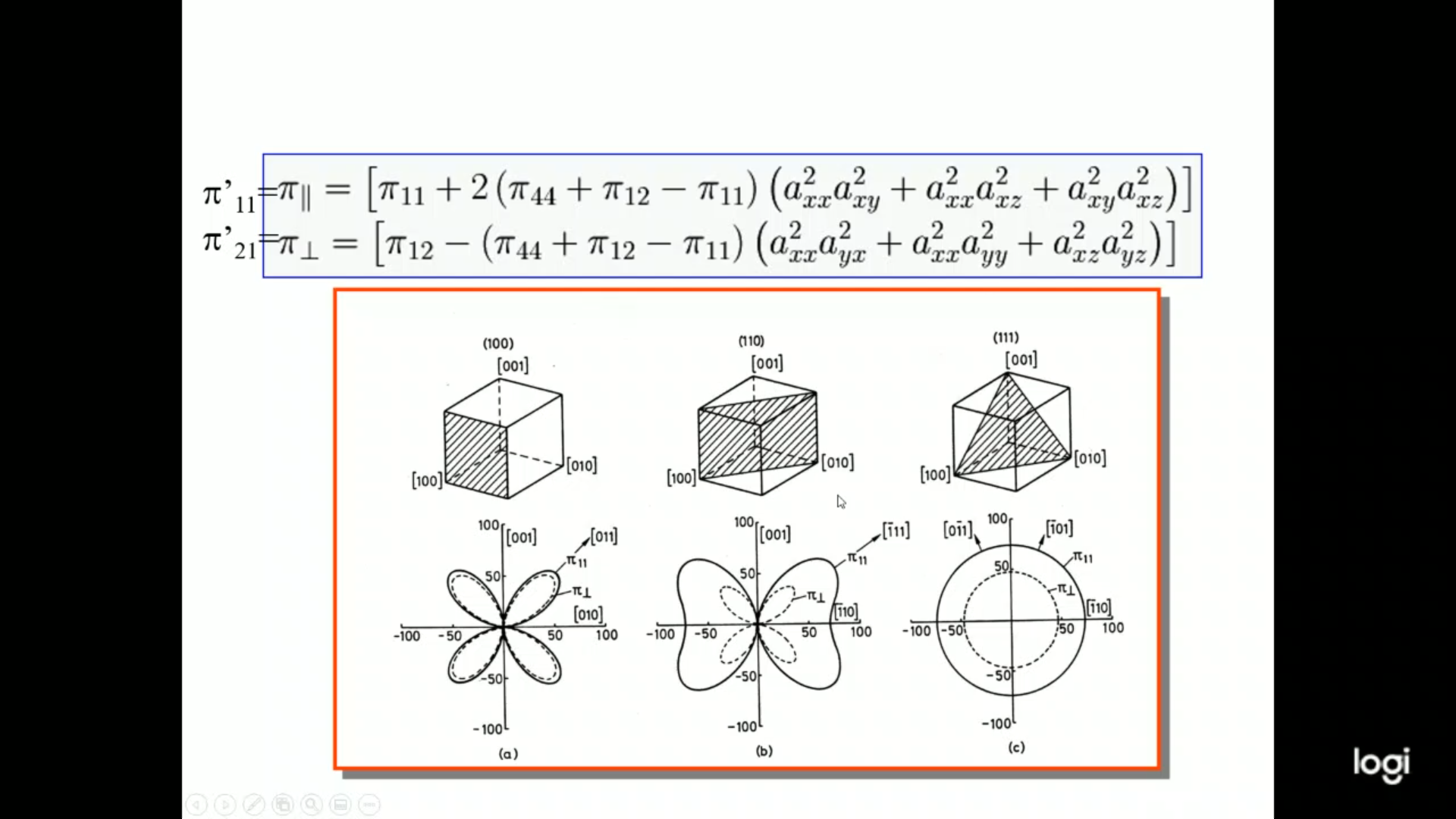
- This is a special chemical reaction, which has an ==etching rate dependent on the direction with respect to the lattice of the crystal==.
That’s why it is called anisotropic.
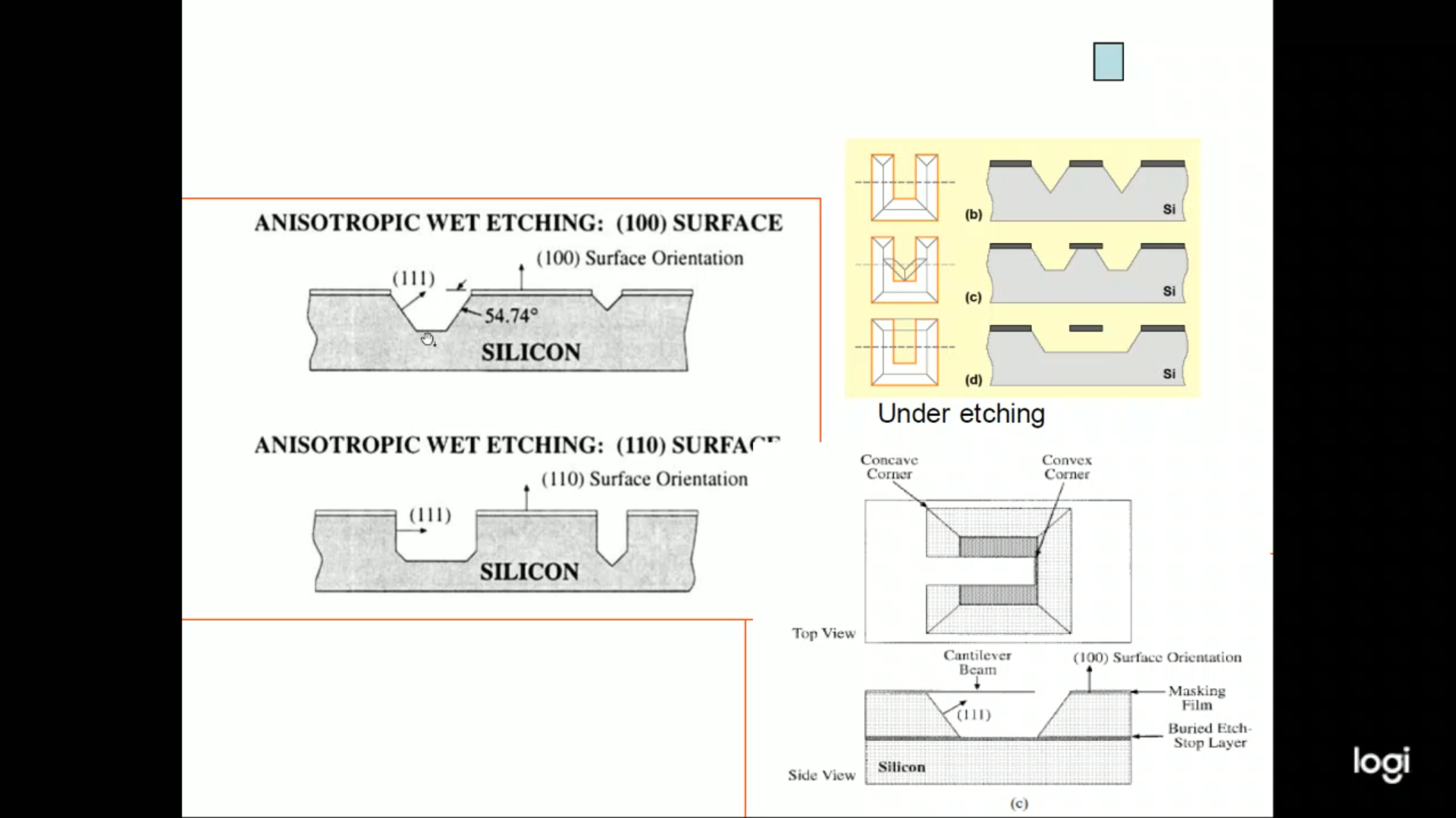
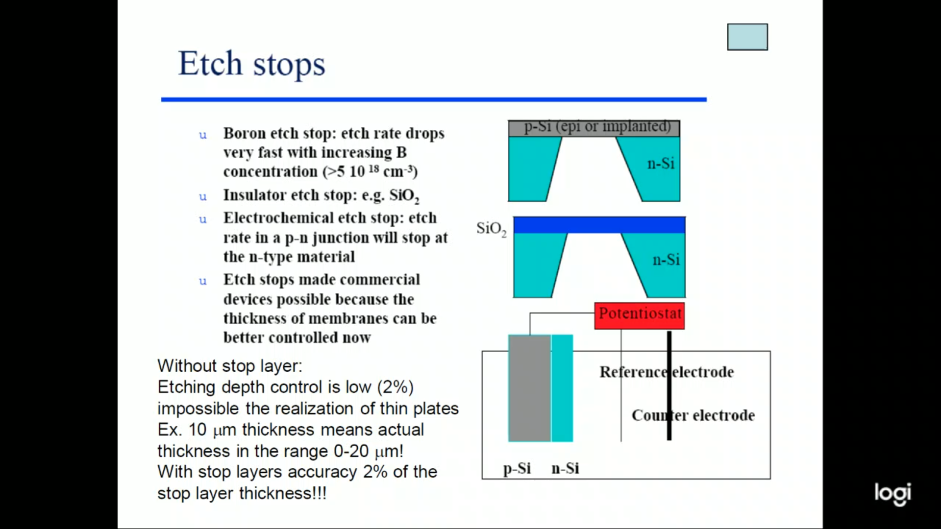
IC - Etch-Stop
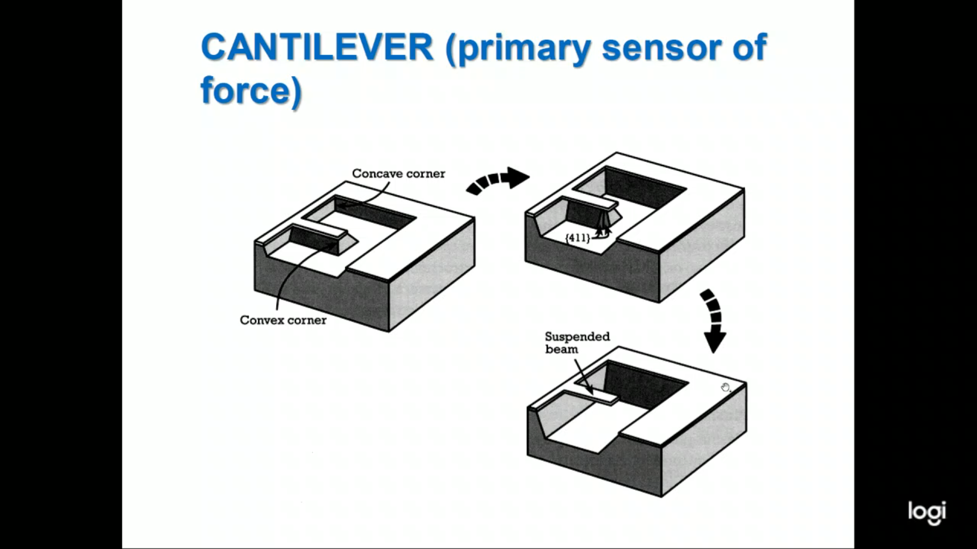
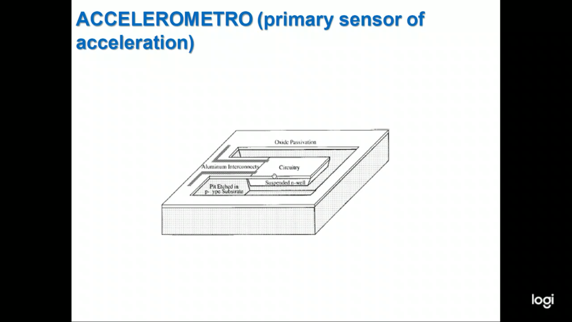
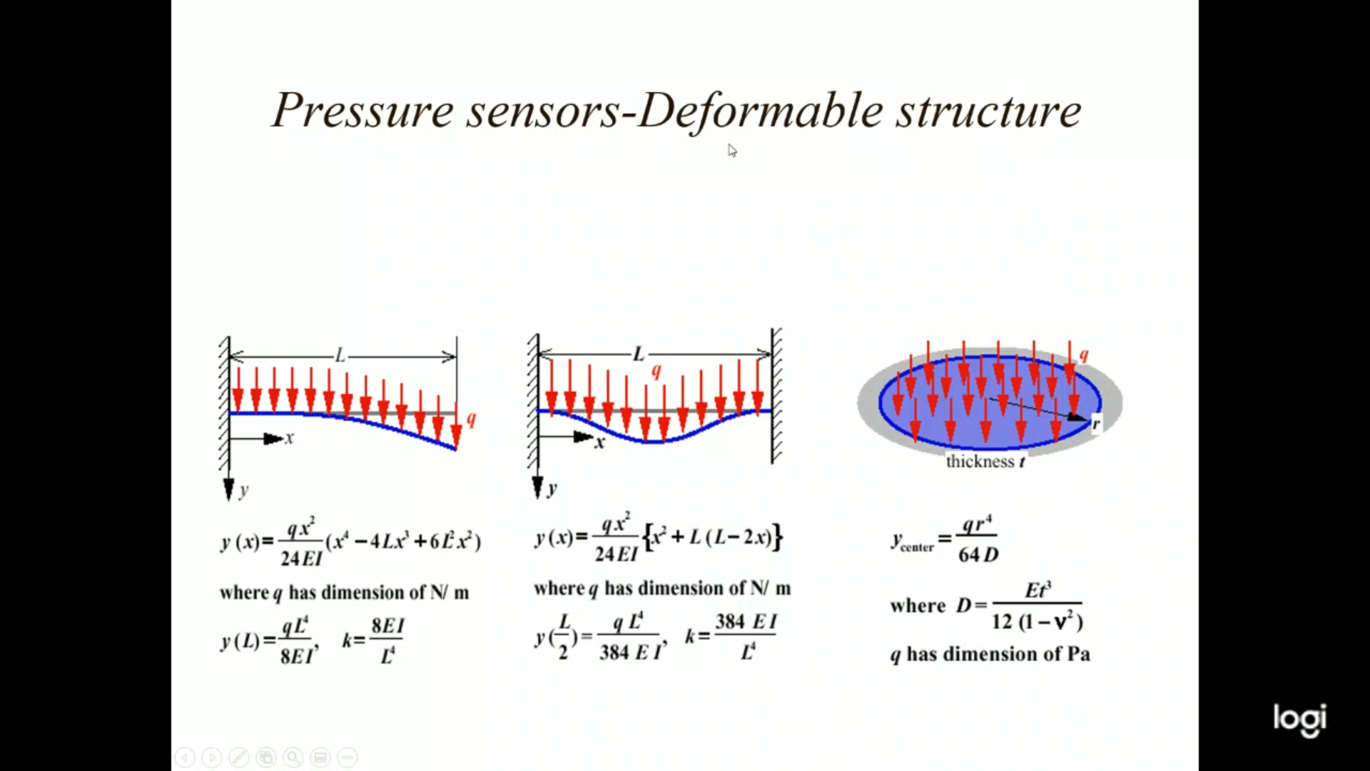
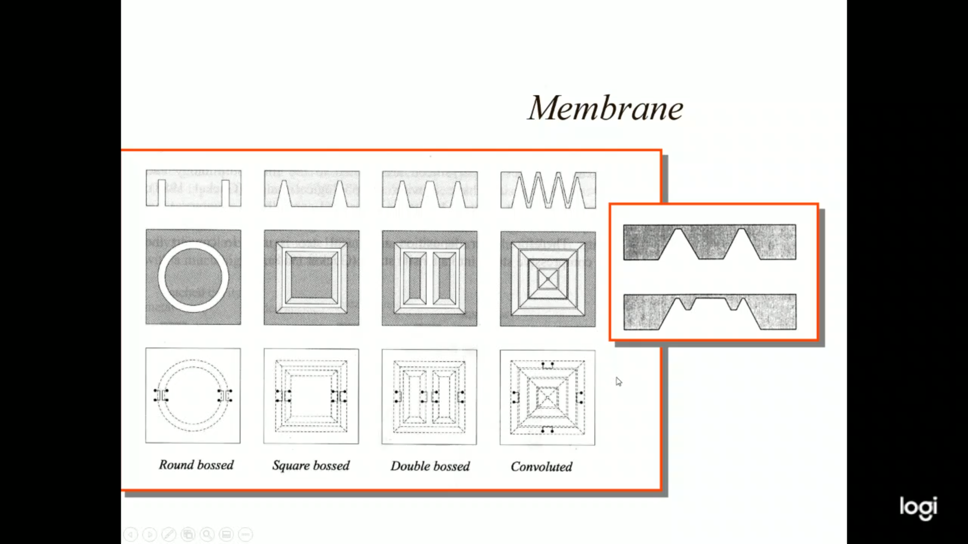
Basic Structures for Bulk Micromachining
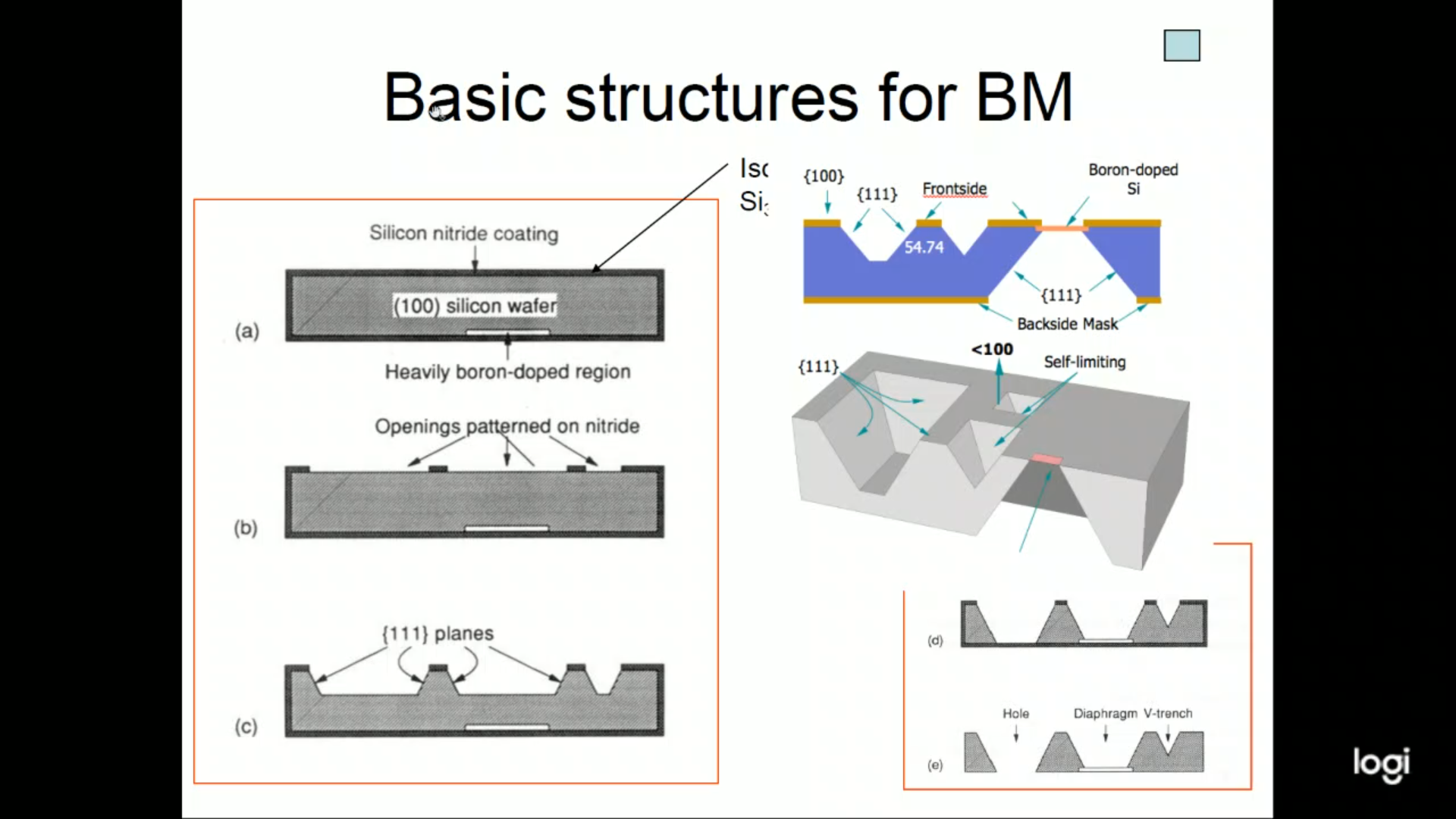
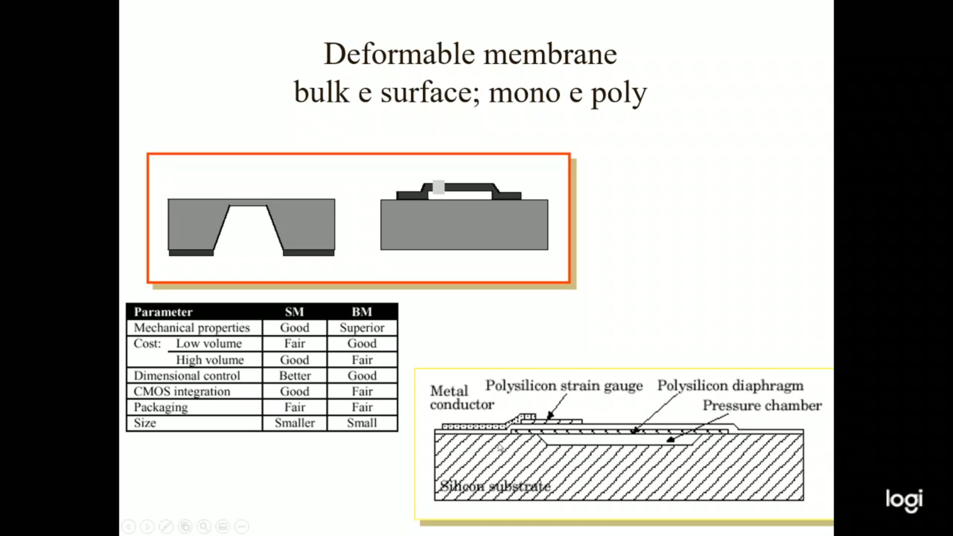
- ==So bulk micro machining is mainly used to obtain membranes==.
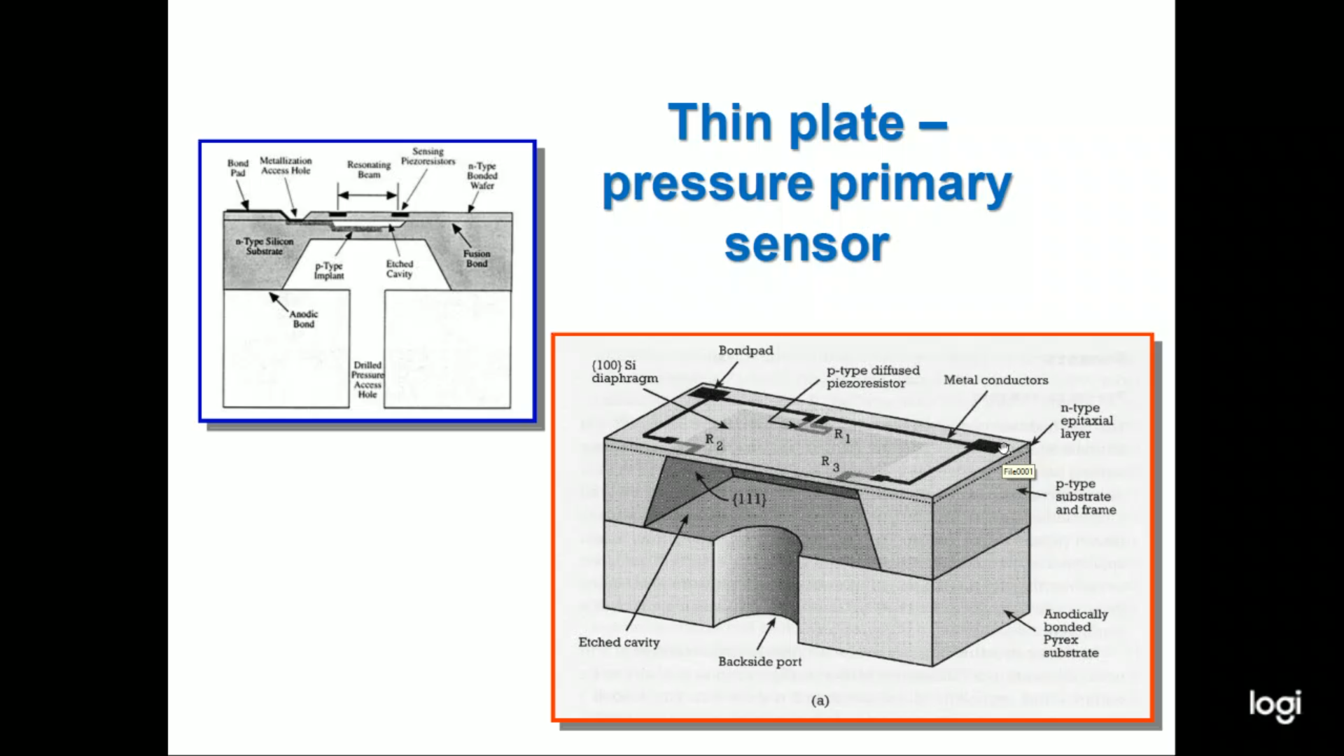
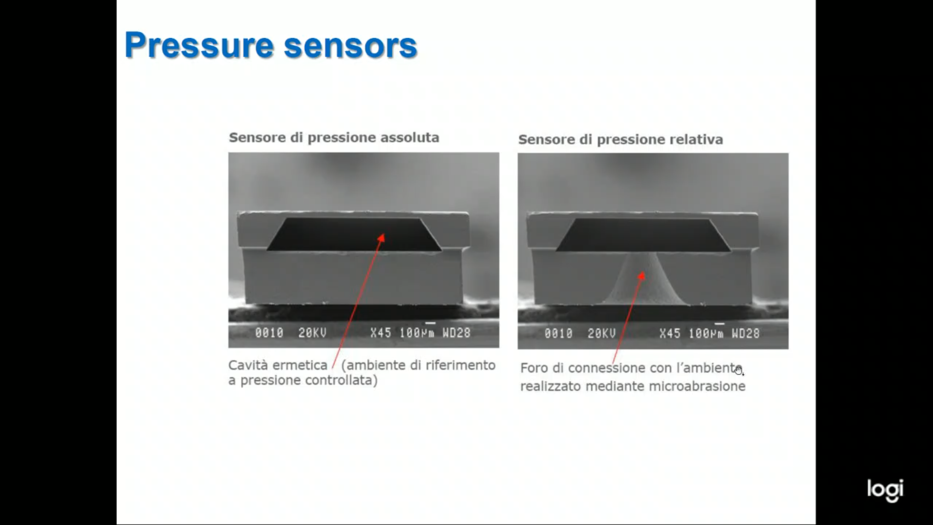
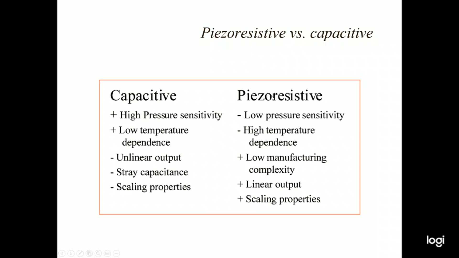
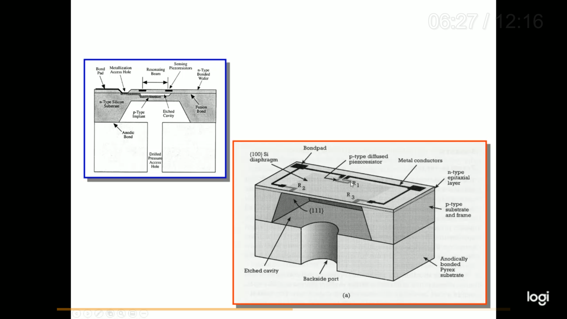
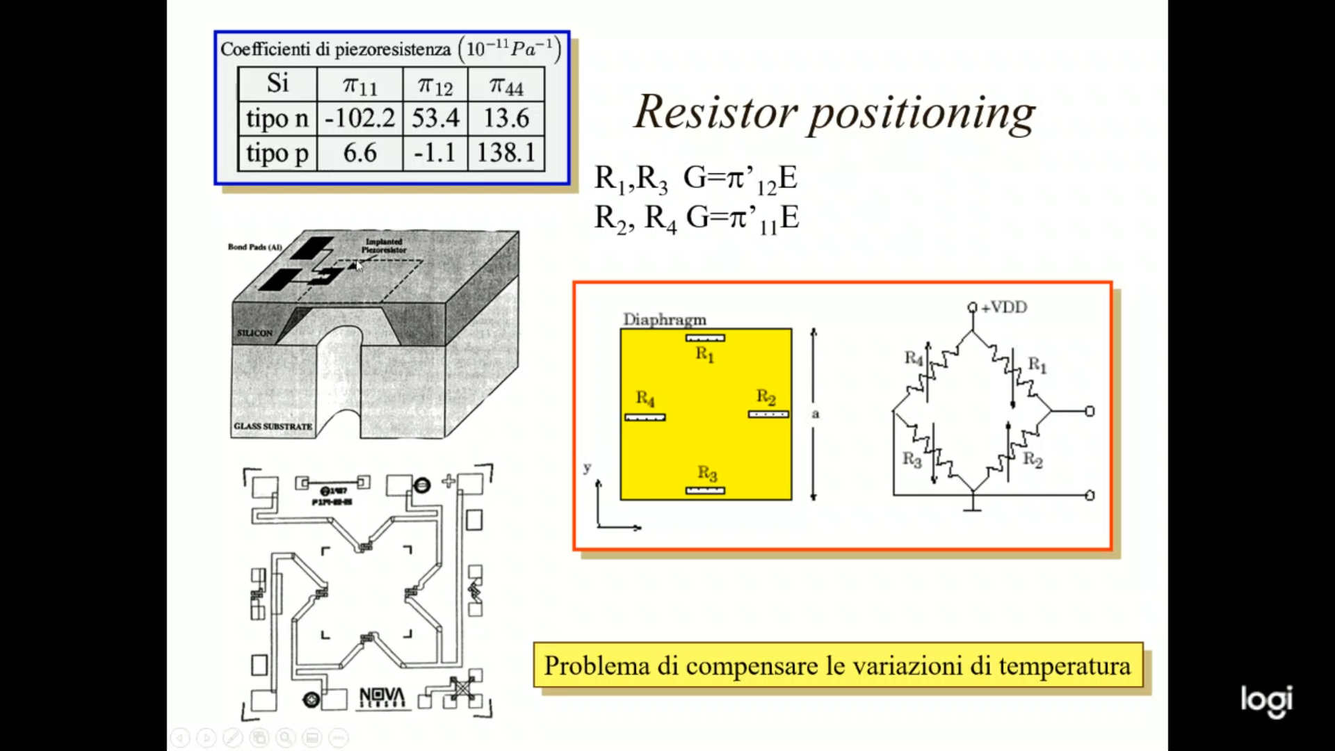
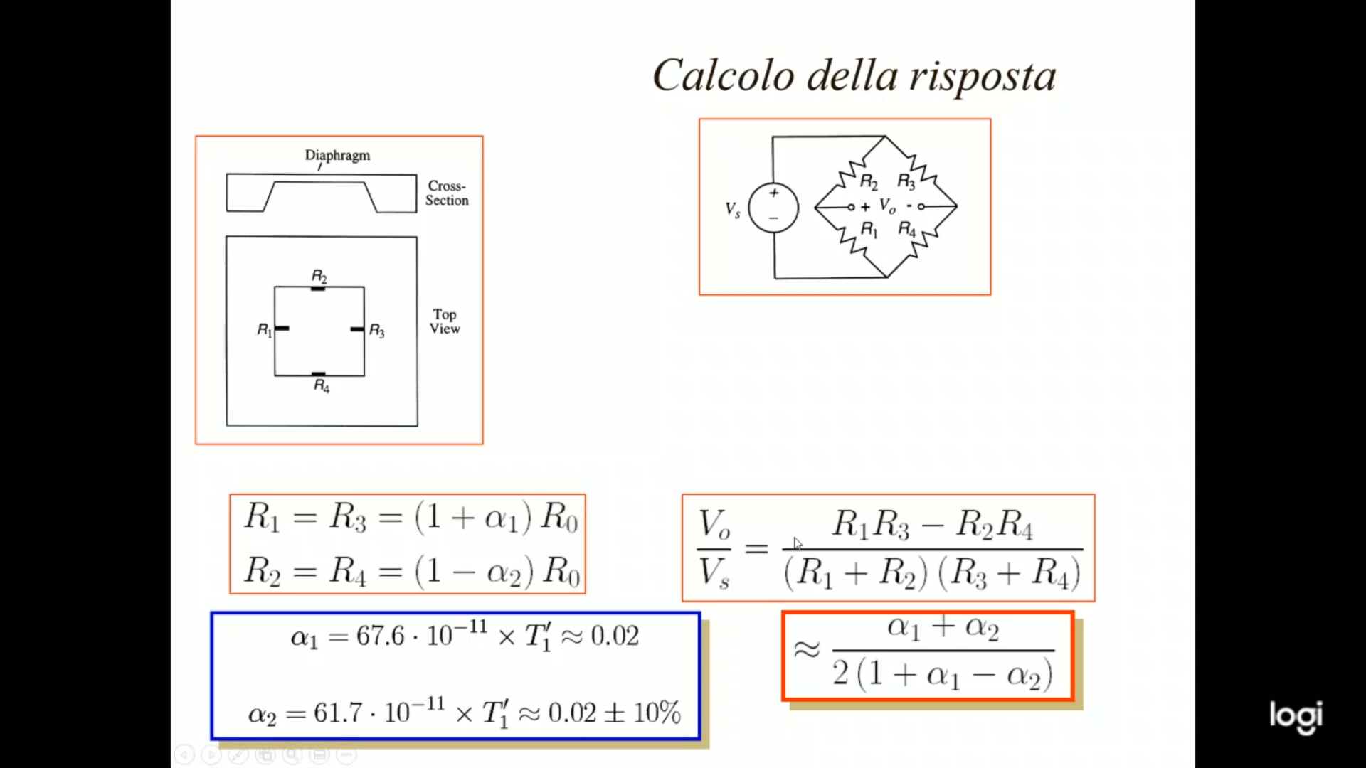
Preassure Sensor
Cantilever
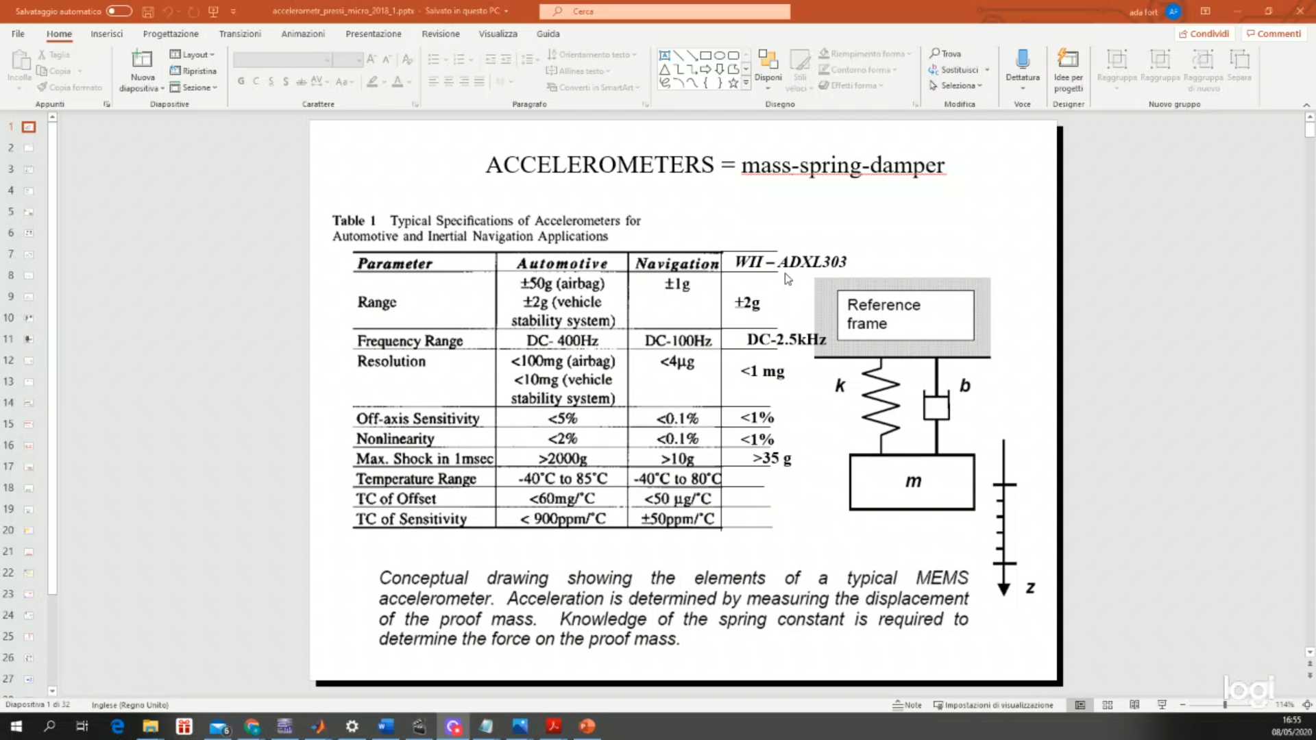
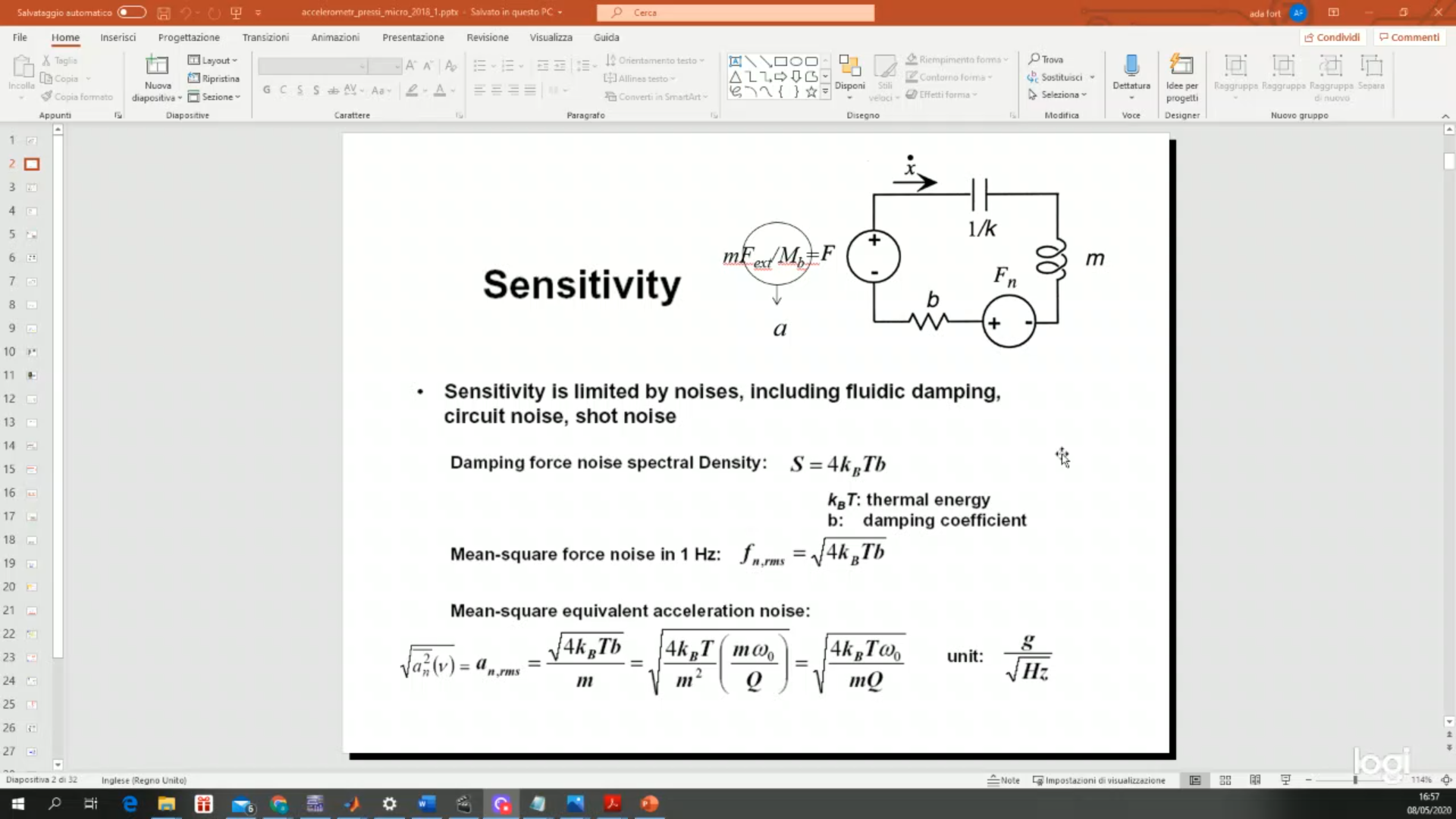
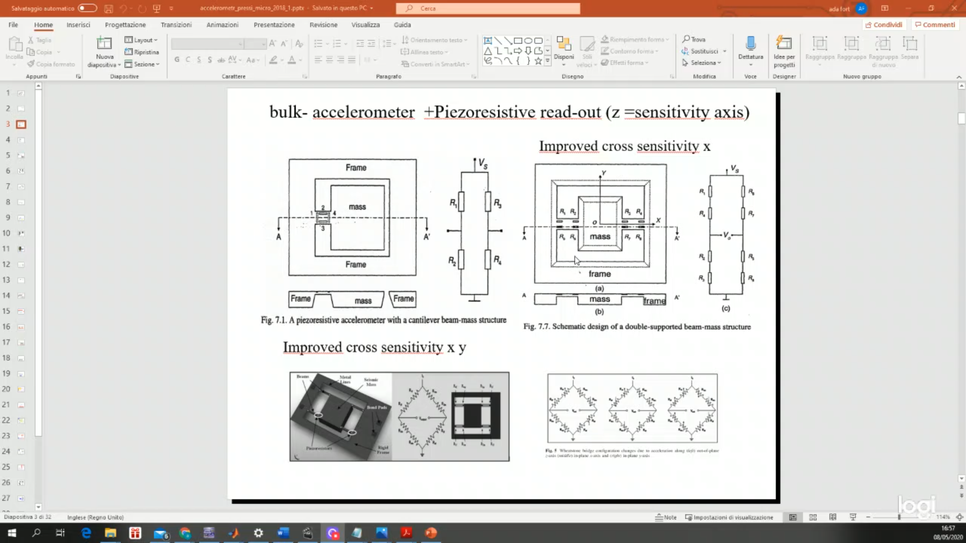
Accelerometer
Surface Micromachining
Surface micro machining instead can be obtained with two types of processes:
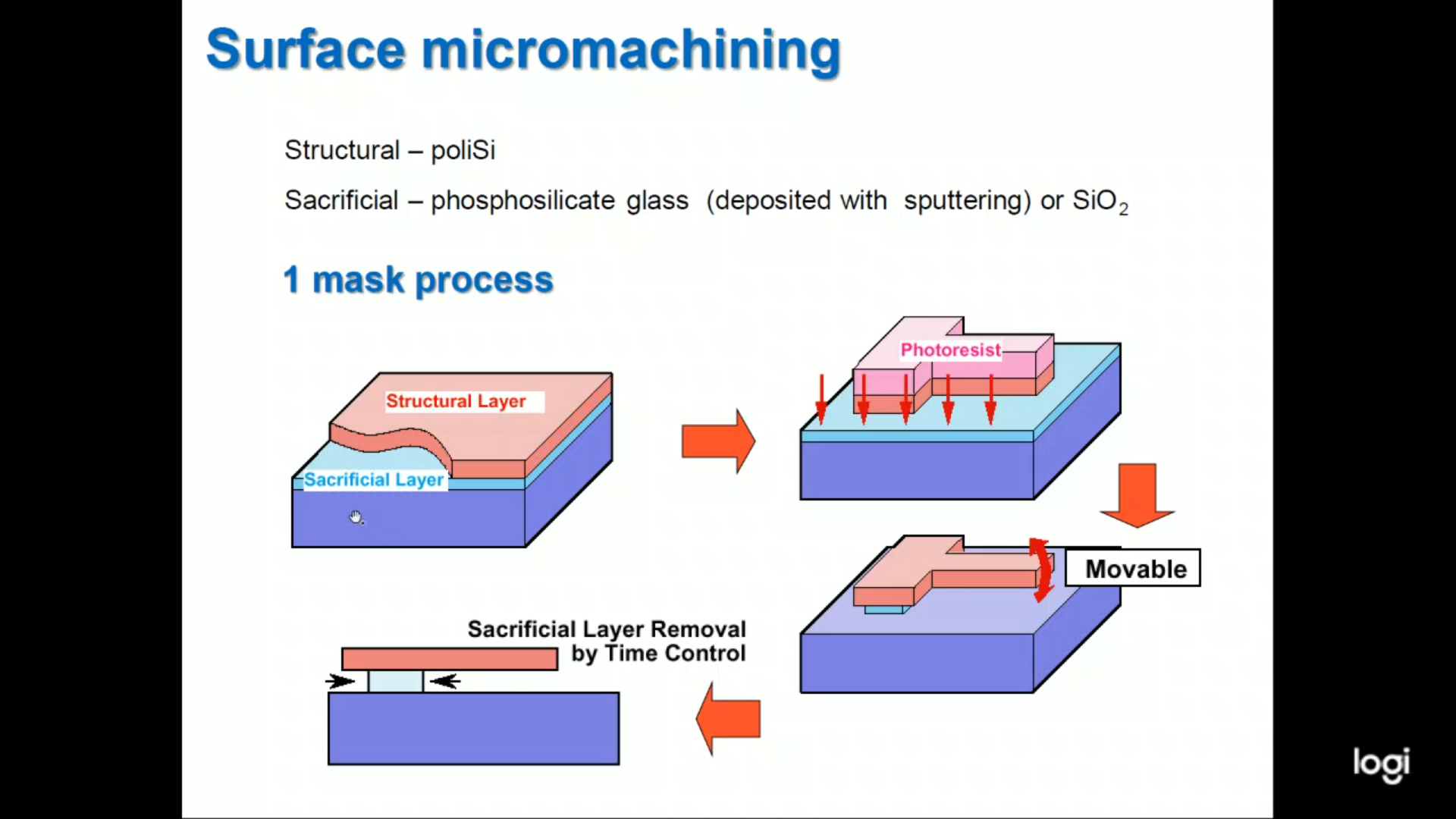
- One is called “one mask process” and it’s very simple, as you can see.
But what happens if the process is not well controlled in terms of time?
Maybe sometimes the encore is lost because there is the complete etching of the sacrificial layer or maybe it is too large and so the dynamics of the sensor is not so controlled.
⇒ So we arrived to the two mask process which has a better control of the “anchor”.
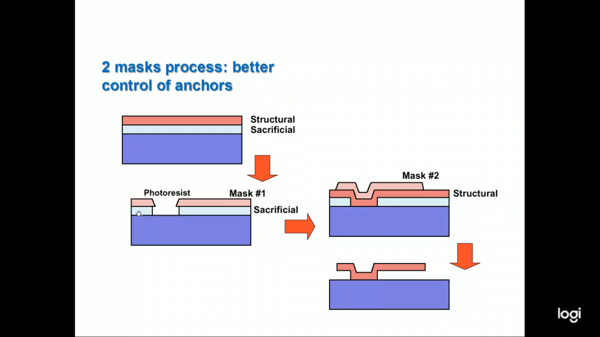
- In this method, only the sacrificial layer is deposited then it is masked.
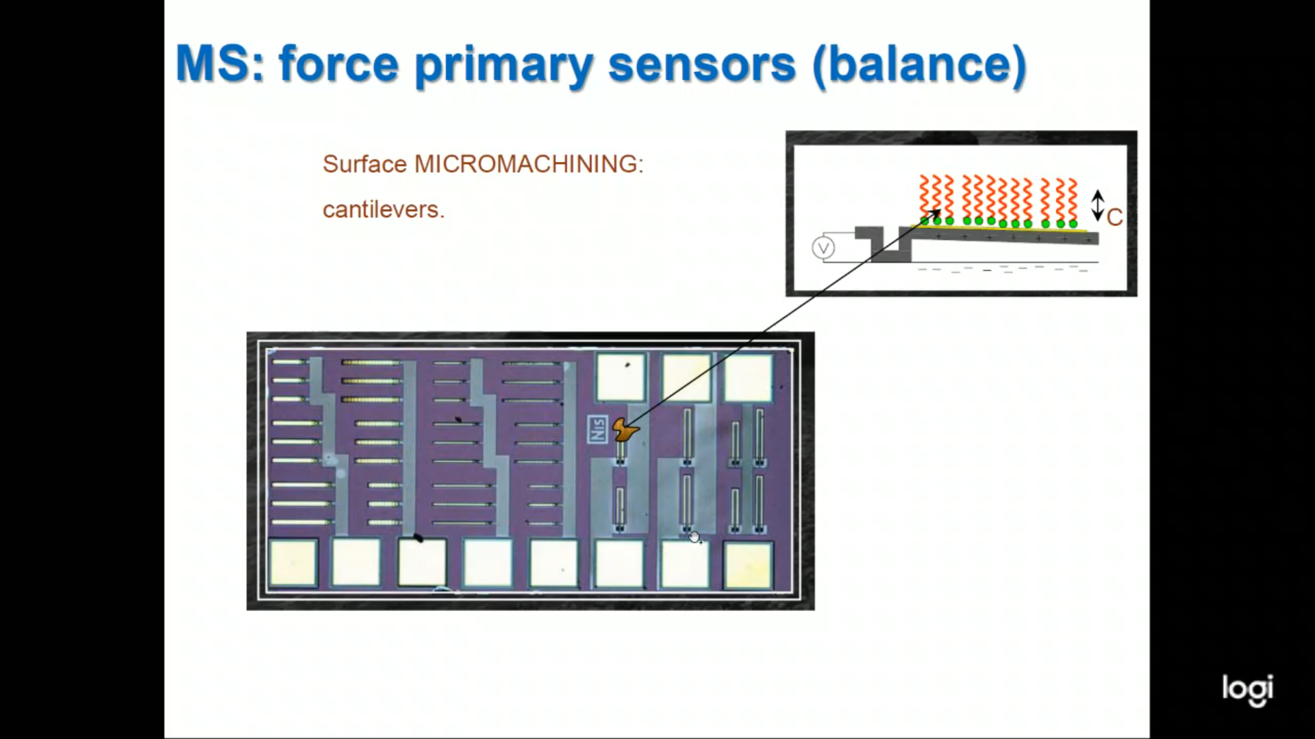
Force Primary Sensor (Balance)
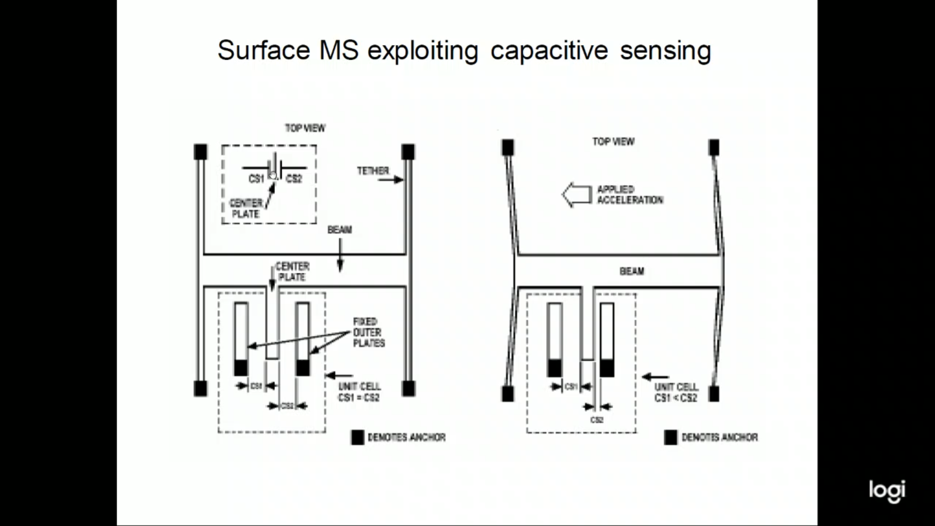
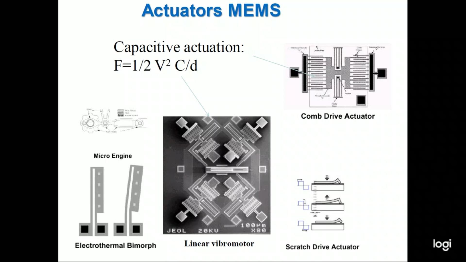
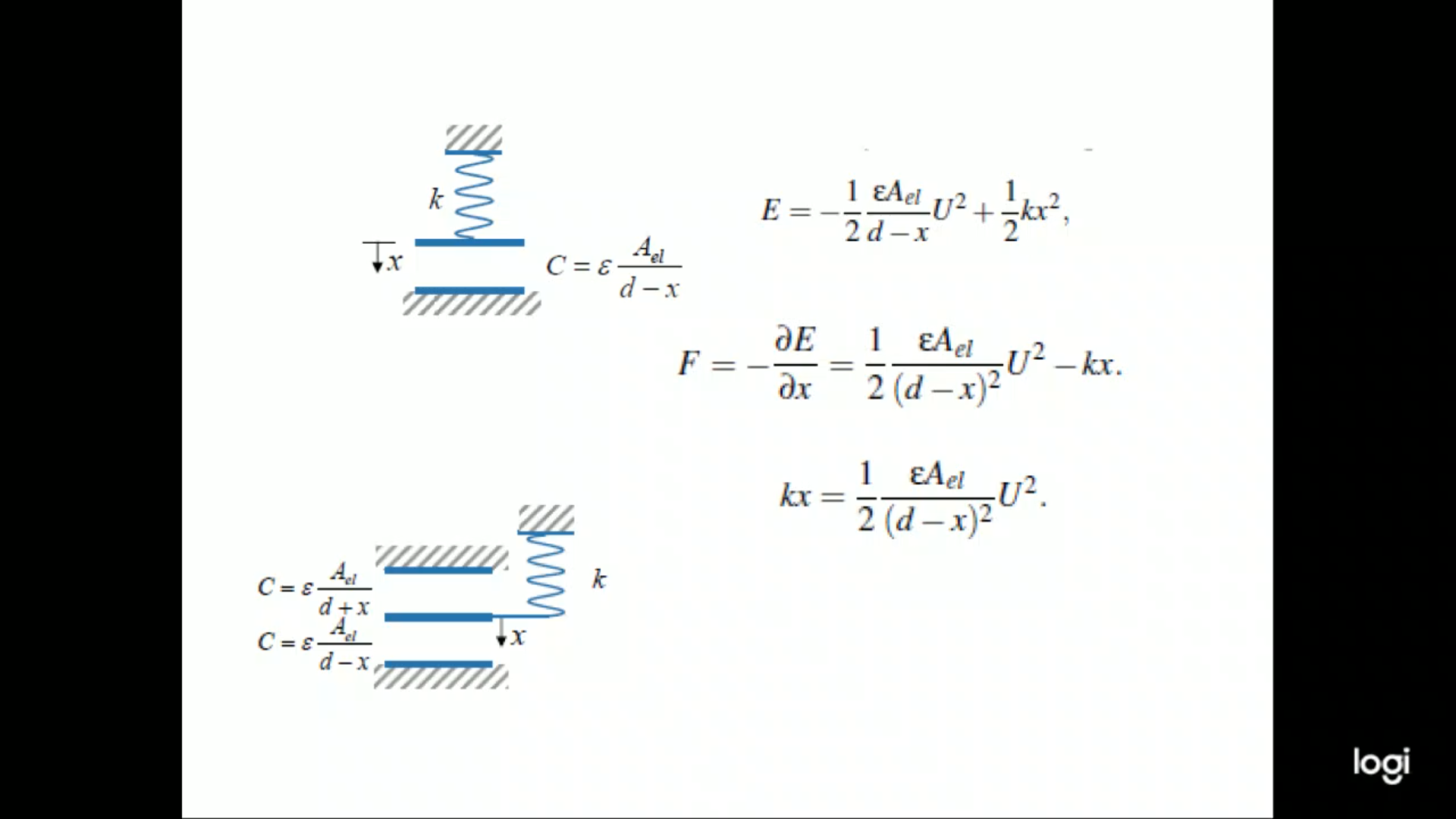
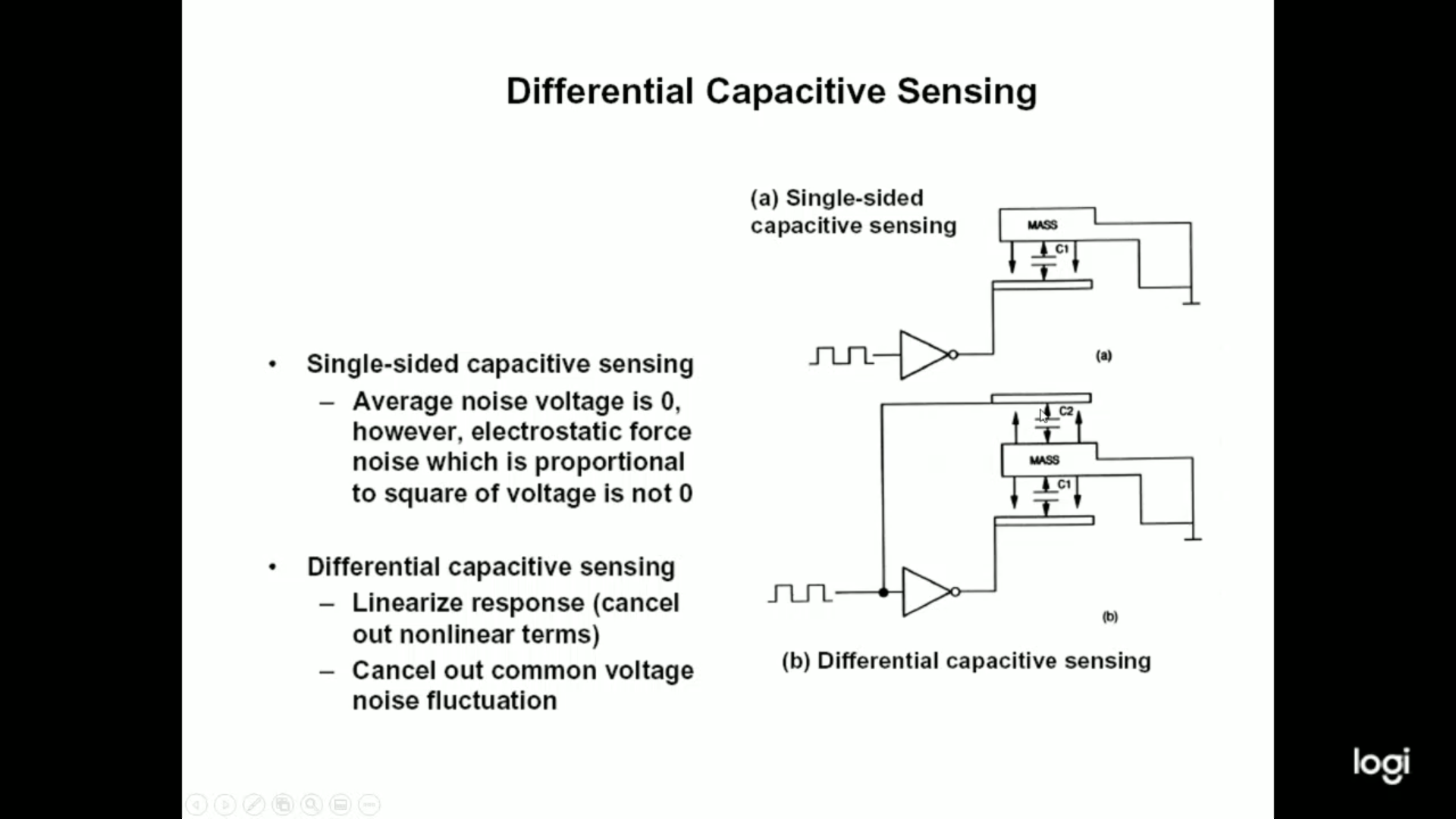
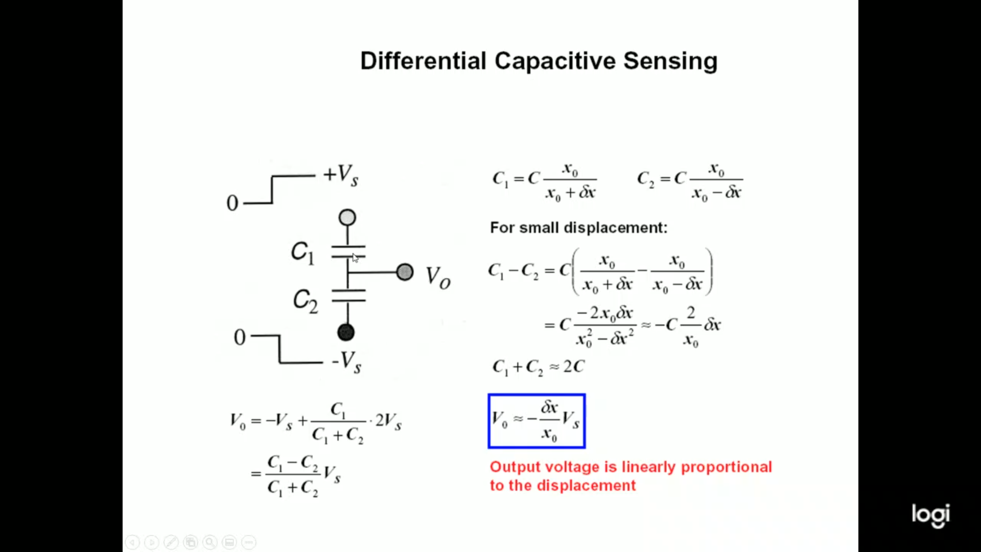
Capacitive Accelerometer
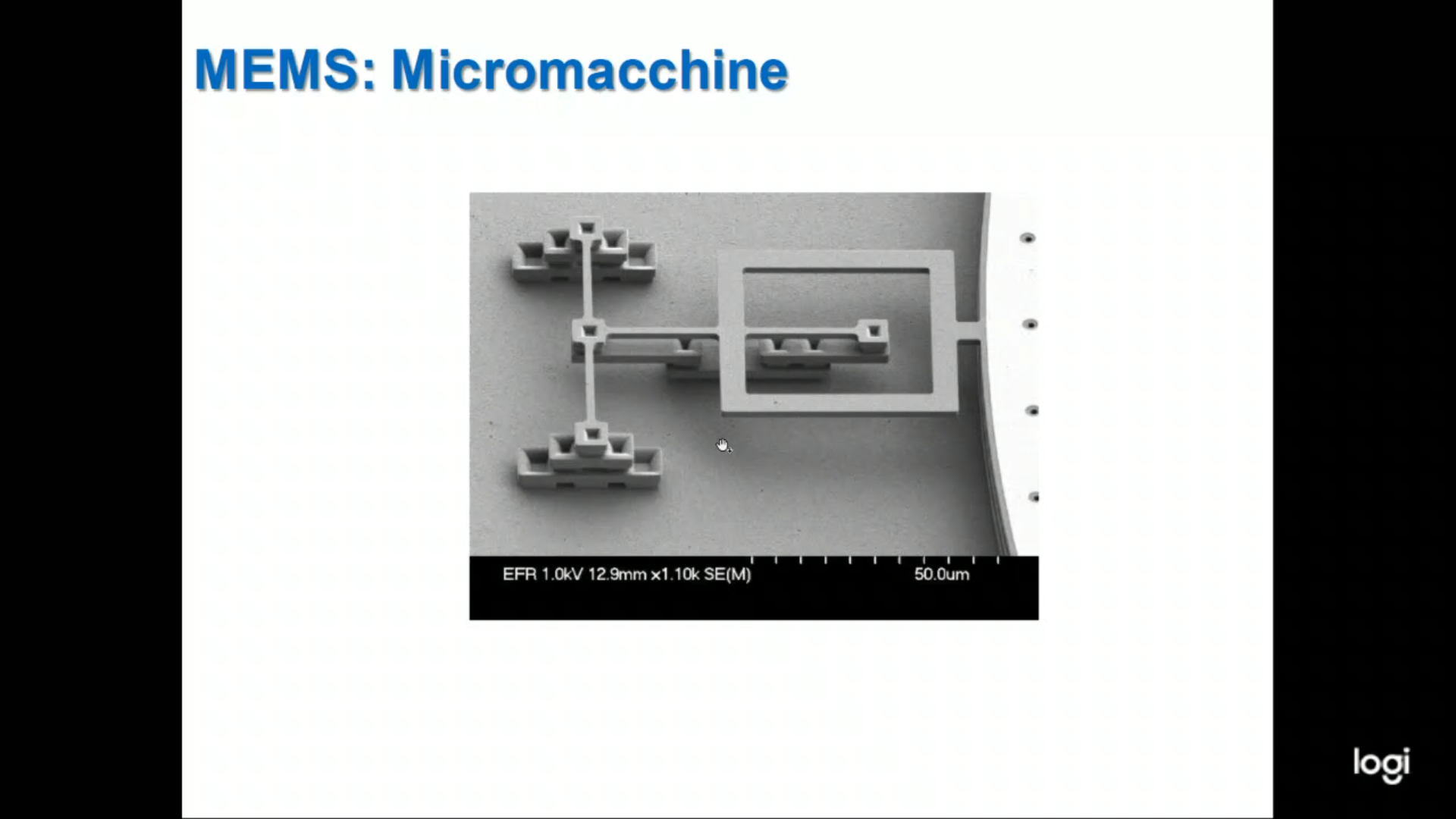
Complex Micromachine
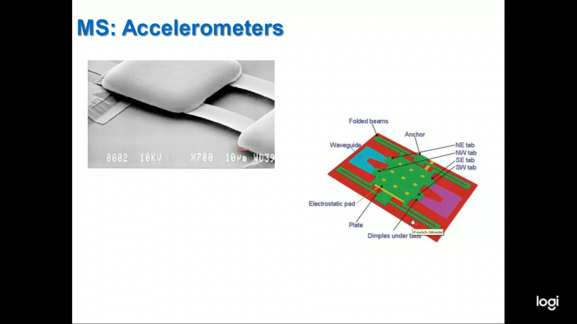
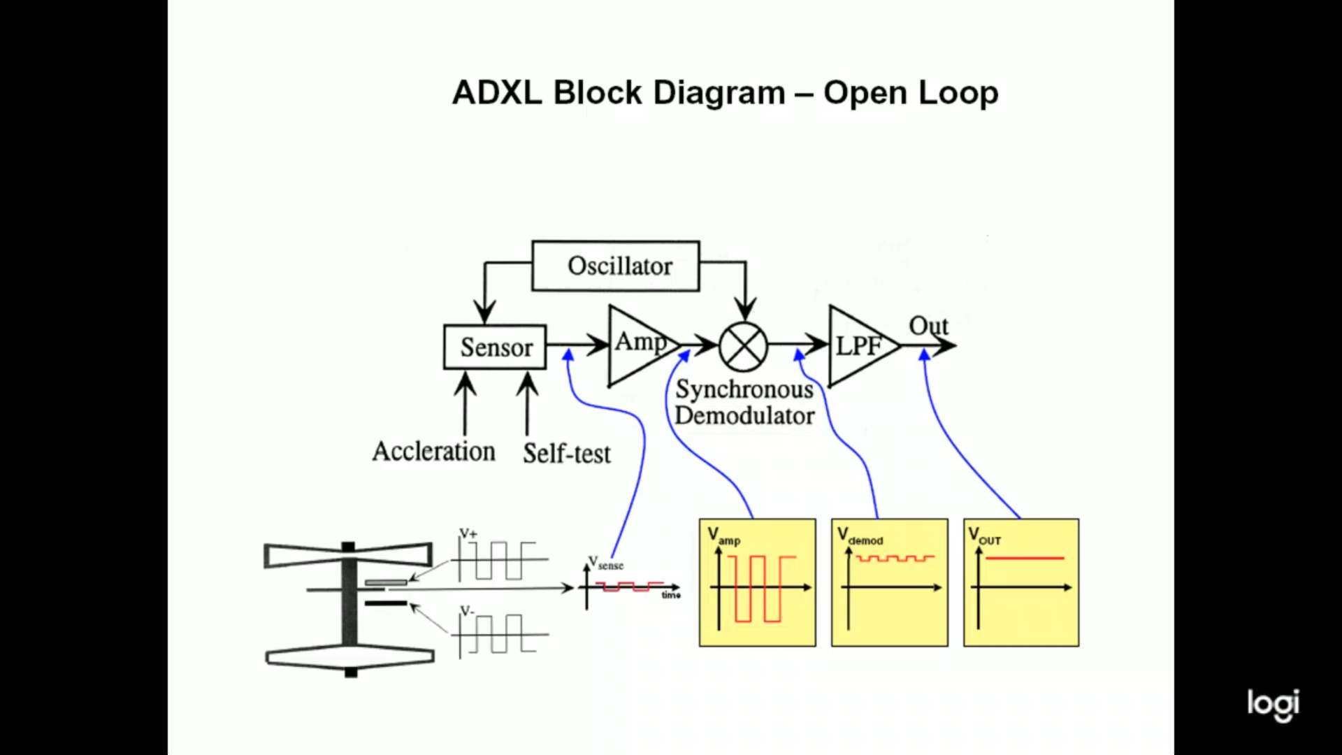
MEMS - Accelerometer
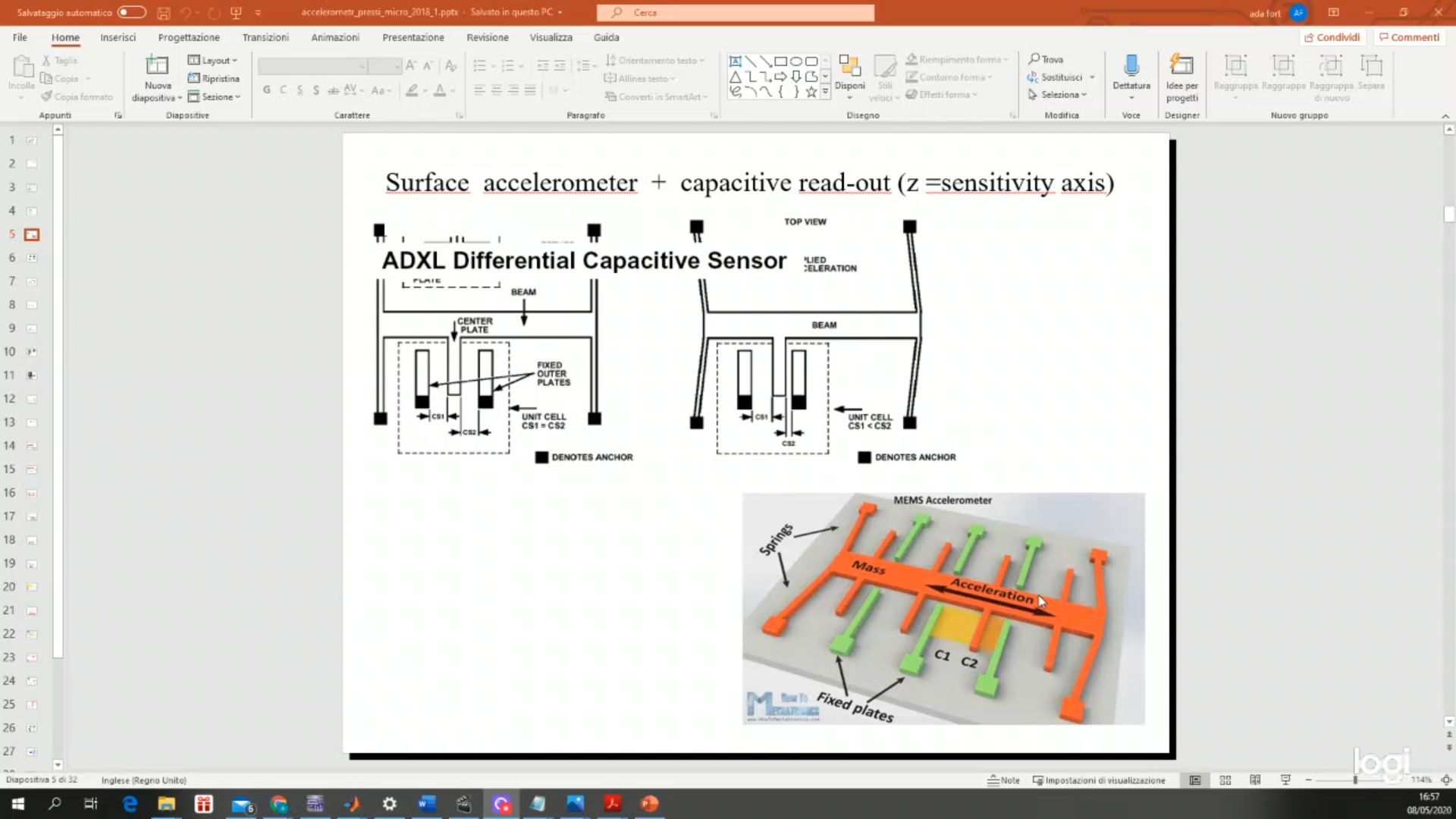
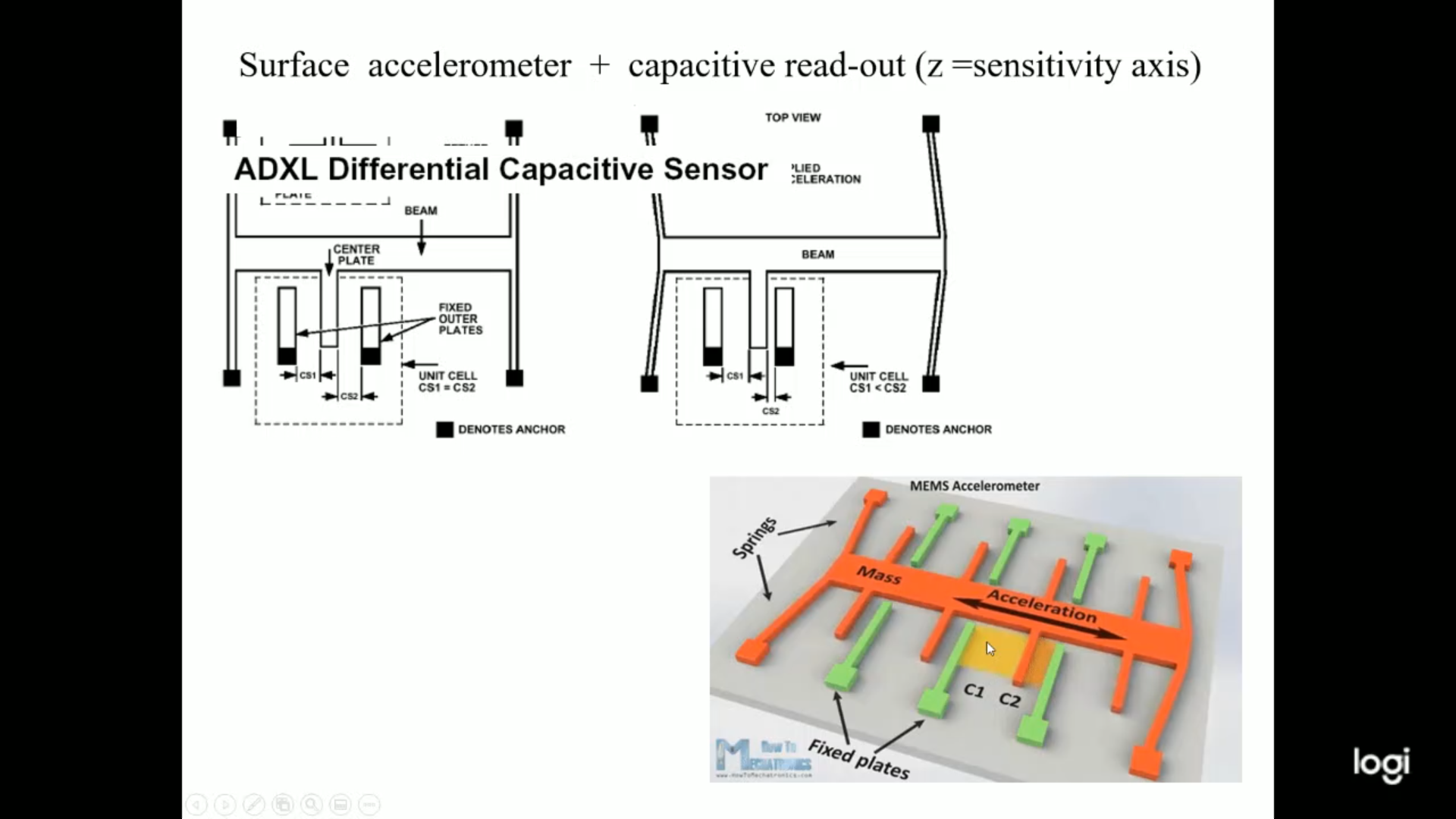

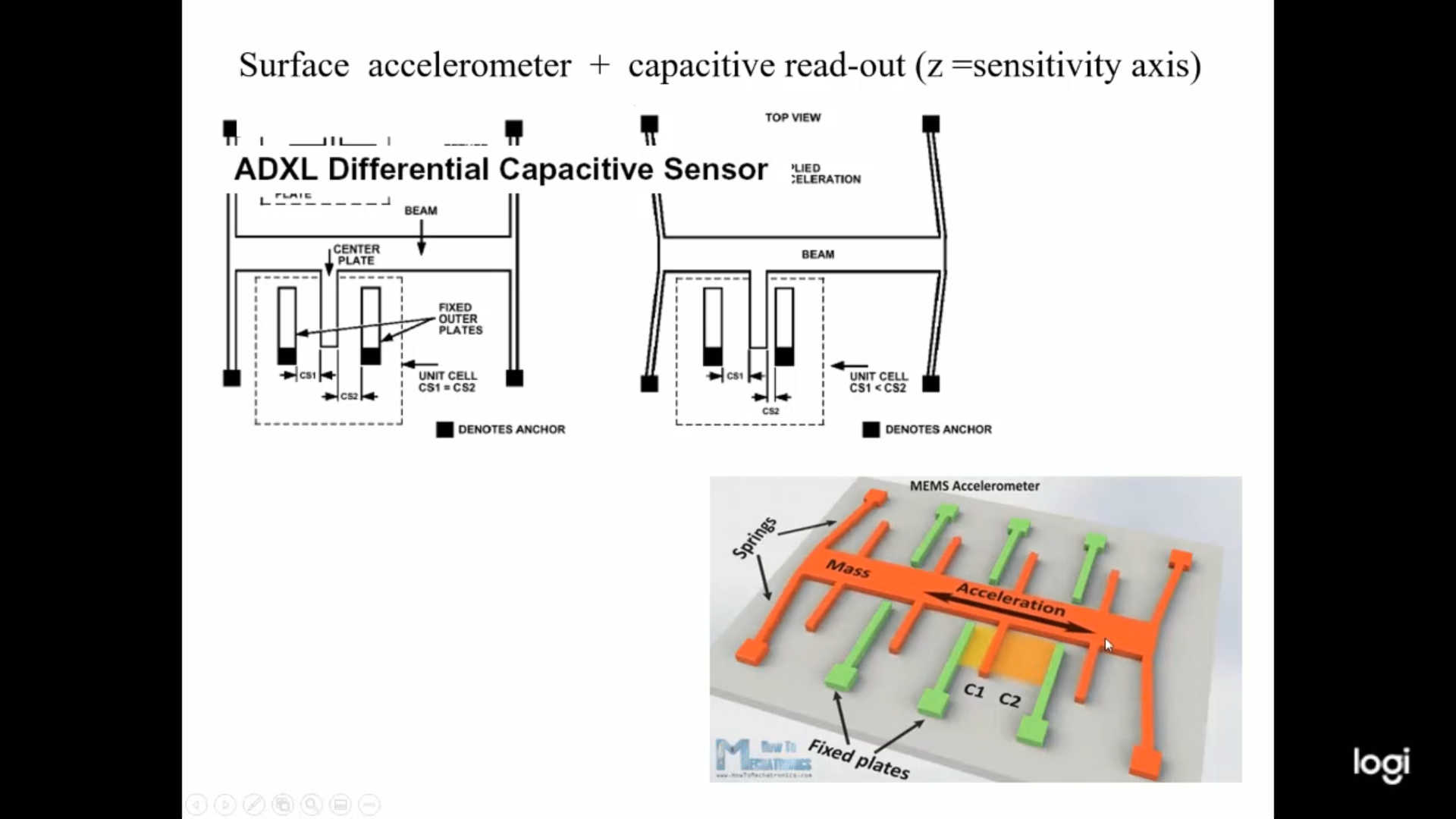
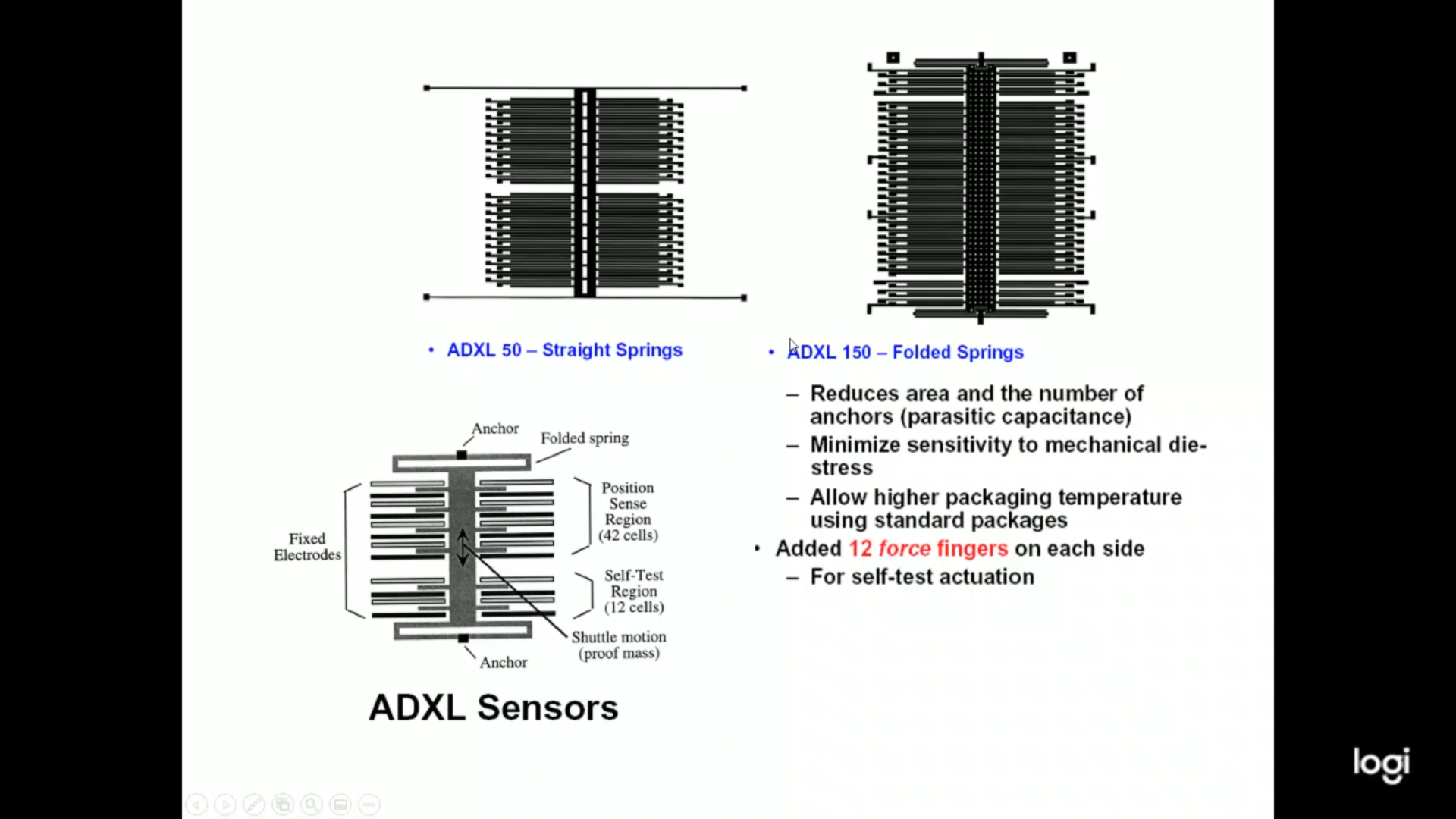
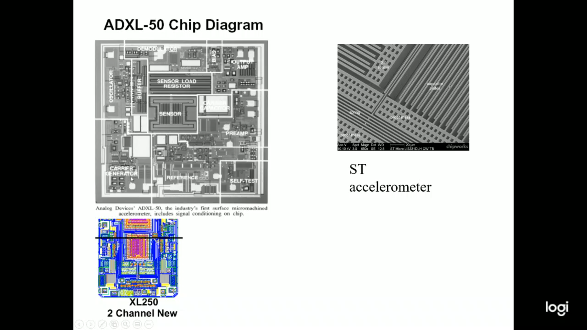
MEMS - Accelerometer Chip View
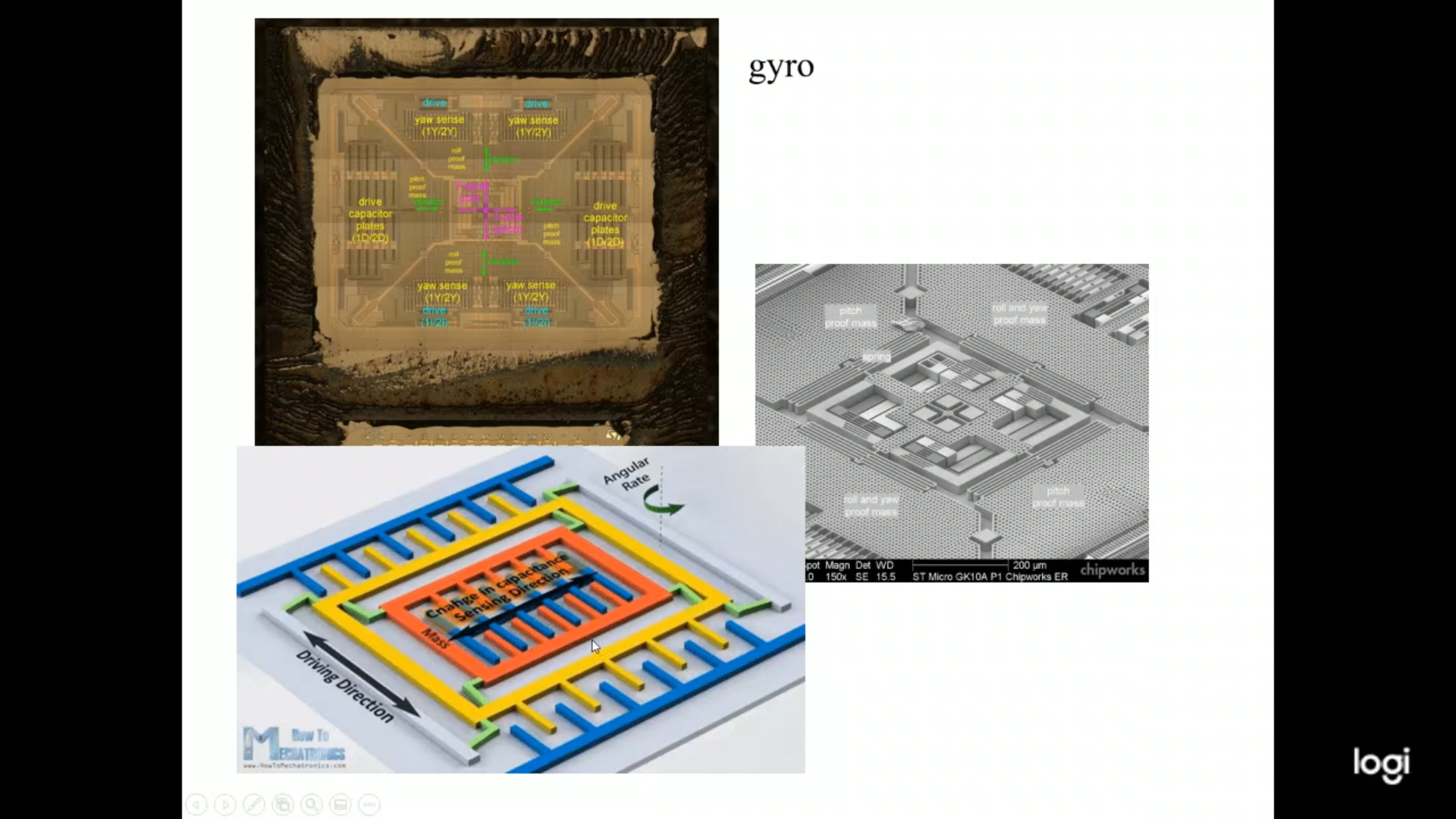
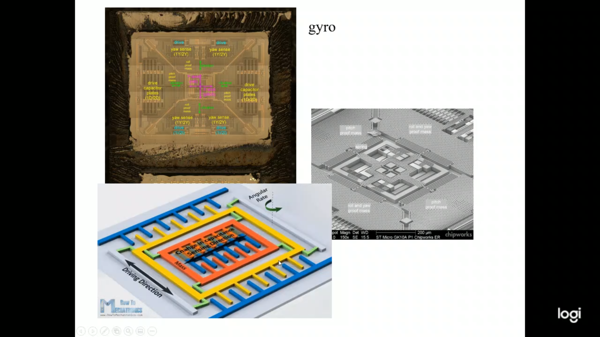
MEMS - Gyroscope

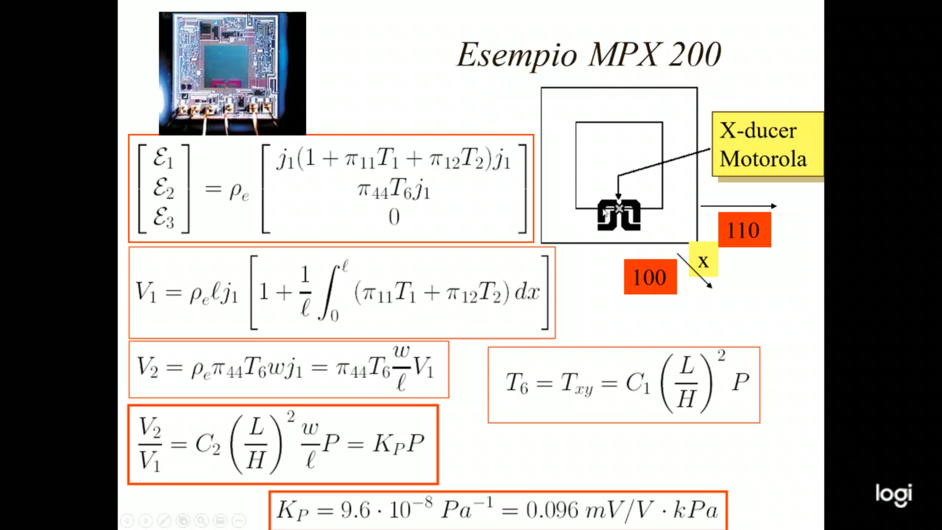
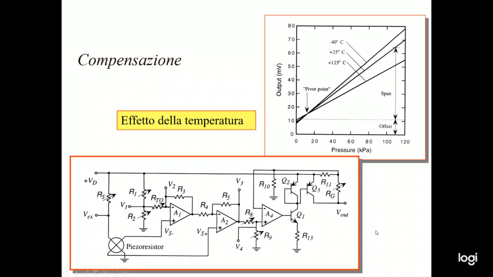
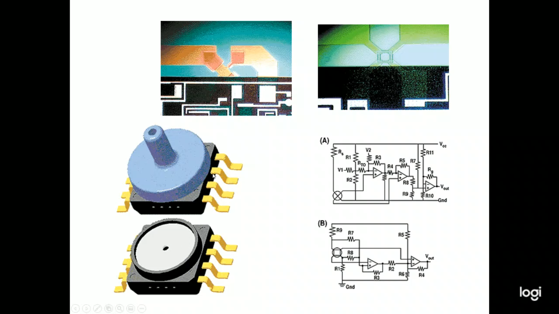
MEMS - Pressure Sensor (Lecture Recap)
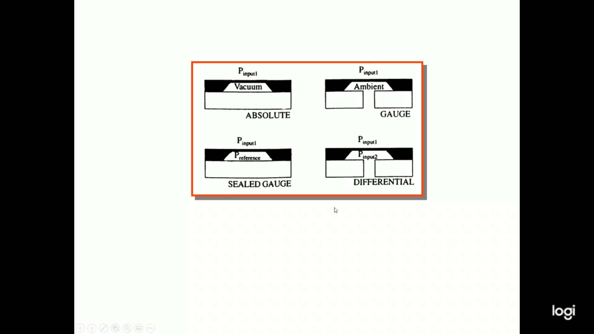
This is what we have done during the lesson:
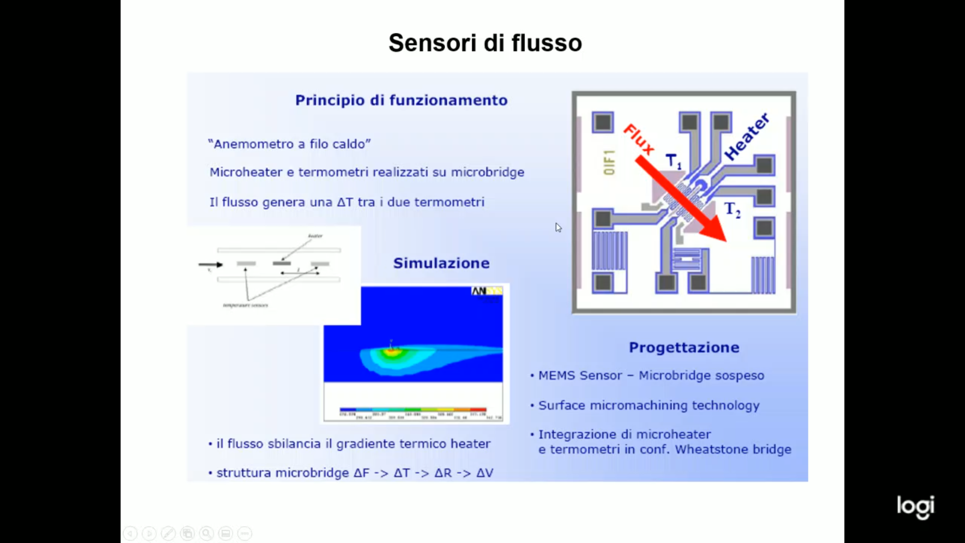
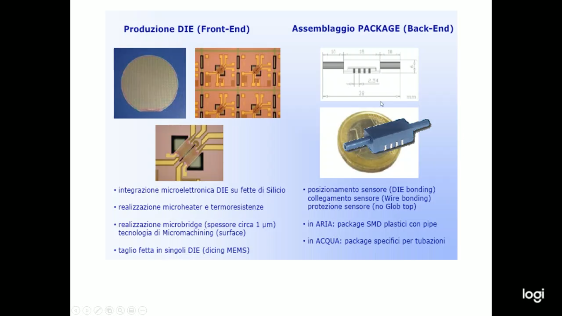
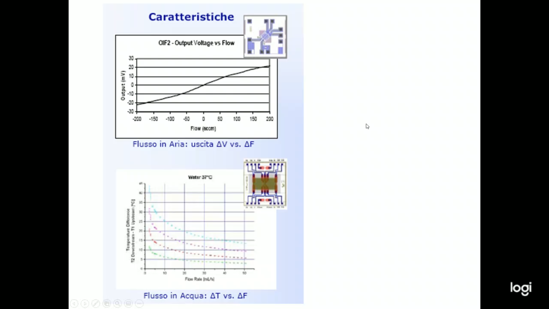
MEMS - Flow Sensor
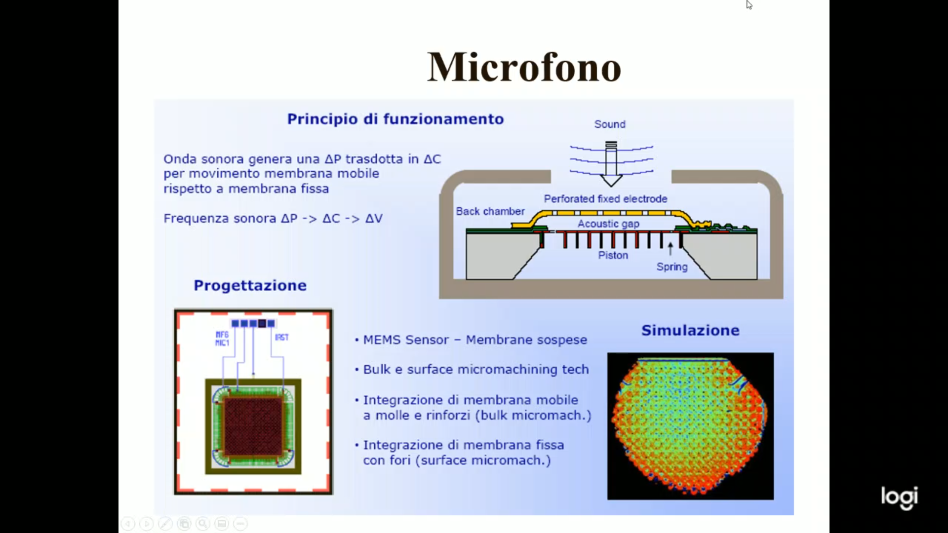
Microphone
Where to Find Accelerometer (Real World Vendor Site)
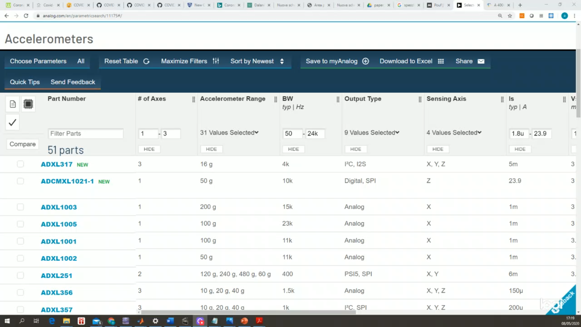
- The most important one is that the front end is close to the sensor, so minimizes the influence of noise.
- The prices are very low, because mass production is possible and therefore the prices can be really more compared to what we can find with traditional sensors.
That usually are more expensive because the production doesn’t allow mass production.