Remeber:
==This is more like a detector than a real sensor, because it usually doesn’t show large accuracy, but it’s a sensor which shows, instead, very high sensitivity, low selectivity== Selectivity in this case means: “which chemichal compound we can detect”.
The output is a resistance, which is a function of this concentration, so . : could be oxygen, it could be nitrogen dioxide, it could be carbon monoxide, …
The sensitivity:is higly non-constant, so this is a non-linear sensor. Also as we have said these are non-selective devices, in fact for a different compound than the one we want to measure, we have:A selective device would have .
This is an active sensor, so it requires power to operate, the power of the overall device can be calculated as:Where:
- : power of the overall device.
- : conductance.
- is the current we feed it.
- We can instead calculate the power as a formula of the temperature we need it to reach, se we measure .
And usually the temperature range is relatively high: .- The reason why it is necessary to bring this resistive sensor to a very high temperature is because the chemical reaction are faster at this higher temperature, which are needed to get the variation of the resistance.
A chemical reisistive sensor is made of:
- Thick film ceramic resistances:
- It is usually ceramic, ==so, it is inert==, meaning it doesn’t interact with chemical compounds.
- Its thickness is usually around micrometers, thats why we call it thick film.
For a thin film we mean having a thickness of less than micrometers.- Two metal electrodes.
- An active layer:
- It’s the material which builds up the sensing device.
Usually, this film is not properly ceramic, because it’s made up of many different grains, so like powder which stays together.- It has a lot of pores, so that gas can reach all the film in its whole thickness.
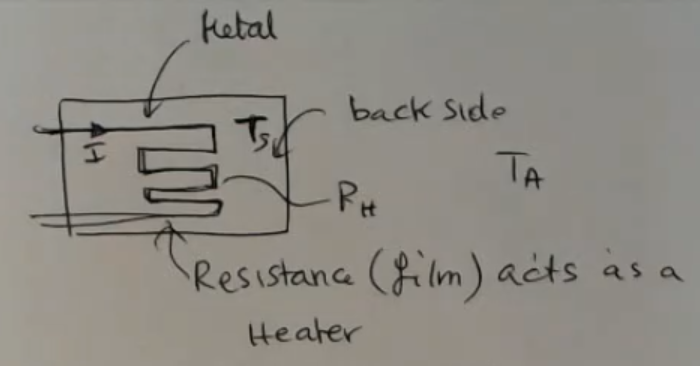
- Thick film metal resisitance (on the backside):
- Acts as a heater (using the current we provide).
Here’s a scheme of the topside:
And backside:
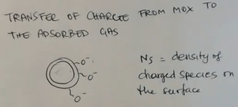
The principle of operation for this sensor here is based on absorption: We take only two grains from the thick film, the current has to pass through these two grains:
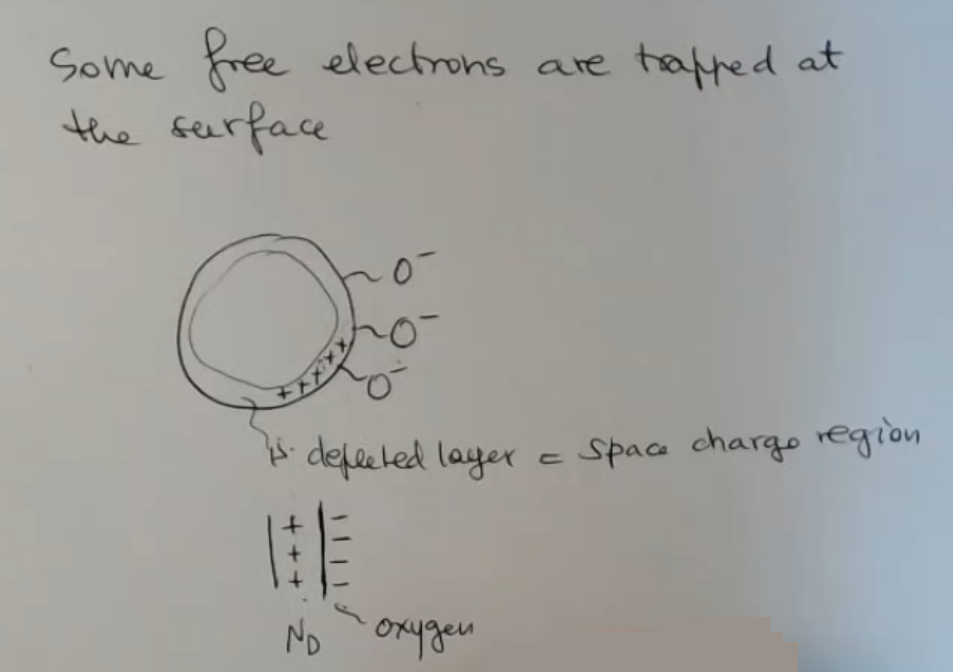
On the surface of these grains here, the gas, which I want to sense, (let’s consider oxygen for instance) is absorbed. After being absorbed on the surface, there is a transfer of charge from the sensor (from the metal oxide) to the gas, and vice versa. So for instance, oxygen tends to take an electron from the metal oxide, and it traps this electron, this negative charge, on the surface. Now I have a charged species on the surface, with a certain density, which I call :
In these metal oxide semiconductors, there are defects which are naturally present which acts as dopants.
⇒ ==So at these temperature these intrinsic semiconductors behave as extrinsic==:Now that I have depleted the layer under the surface, meaning the layer has no electrons, since they have been taken by the absortment compound, which is oxygen in this case.
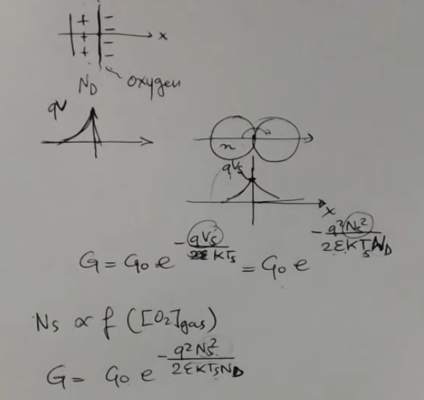
⇒ ==We have a plus charge region under the surface, like in a diode==.So obviously you have a minus charged layer, a positive charged layer, so you have an electrical field, and associated with this electrical field, you have a voltage barrier, like this:
When you place two grains together and you want the current to flow through, at the surface of each grain there is the potential barrier.
⇒ So only the electrons which have enough energy to overcome this barrier can pass through to the next grain, and so contribute to the overall current in the film. This is like a diode, and for this reason at the end, we can find the conductivity of the film:Where:
- : height of the potential barrier between each grain of the substrate.
- : density of the absorbed and charged chemical compound.
- : temperature of the sensor.
- : density of donors.
- : Boltzmann’s constant.
- : electric permittivity
- : electric permittivity of the void
- : relative electric permittivity
Note from this formula:The temperature of the sensor () has to be kept very, very constant, otherwise you have a reaction due to temperature which is of the same intensity as the reaction due to chemical compound concentration.
==The Selectivity of these devices is decided by the chemistry, some materials tend to absorb some gases, others instead other gases==. So by selecting this specific type of material or the dopants put into the material, you can change which kind of gas is absorbed.
Also, ==these are sensors which are not so reproducible==. The processes which happen at the surface are quite not so known. The final equation gives only an approximation of what really happens, and it can be very different on the basis of different material and different microstructure of the field.
⇒ Read carefully the data-sheet.
==One of the most important influence factor is the humidity which is the water vapor, always present in the environment. And also the change of temperature may really change the behavior of the sensor==.
Memory Card
Index
- Chemical Resistive Sensor
- How is a Chemical Resistive Sensors Made
- Analysis of Two Grains of Material for Chemical Resisitve Sensors
- Conclusions
- ~Ex. Data Sheet of a Hydrogen Gas Sensor
Chemical Resistive Sensor
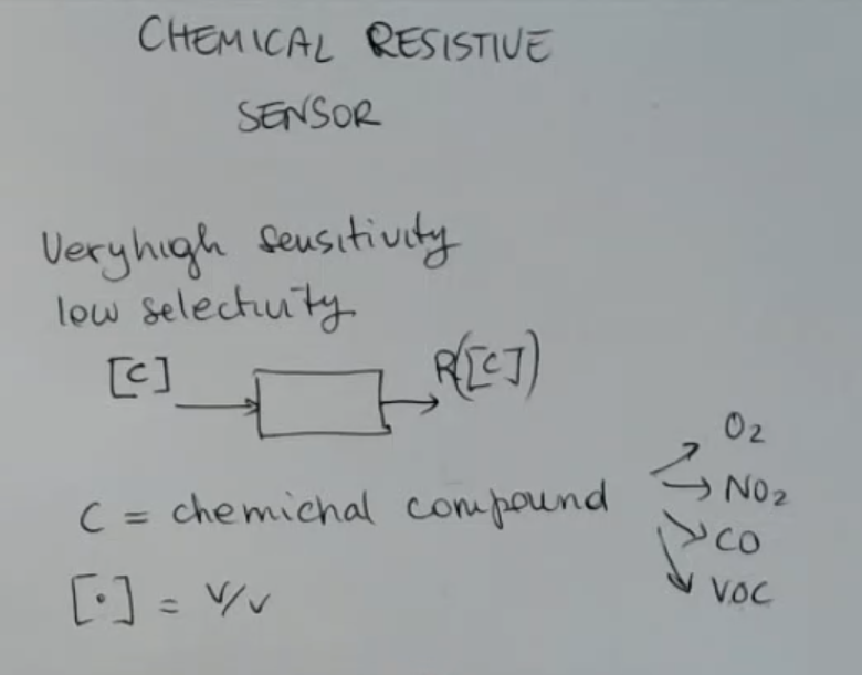
- Sensitivity means that the variation of resistivity is very high, with respect to the variation of concentration.
- Selectivity means “which chemichal compound we can detect”.
- ==This is more like a detector than a real sensor, because it usually doesn’t show large accuracy, but it’s a sensor which shows, instead, very high sensitivity, low selectivity==
- : could be oxygen, it could be nitrogen dioxide, it could be carbon monoxide, …
- The output is a resistance, which is a function of this concentration here.
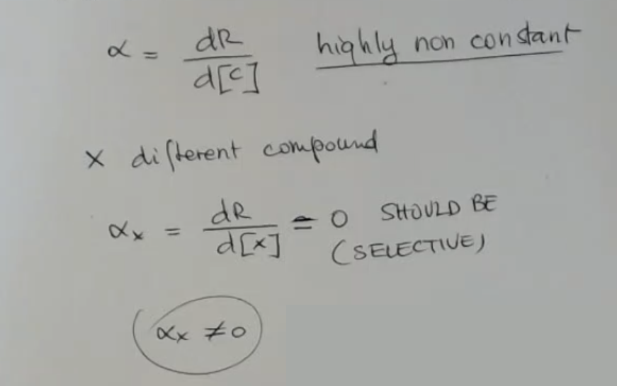
- : sensitivity
- : sensitivity to a differnt compound ().
⇒ This devices are NOT selective. - It’s highly non-linear, non-constant.
So ==this kind of device has no linear behavior==.
Obviously, if as usual, we consider very small range for the input quantity, we will have an almost linear behavior for the output quantity.
How is a Chemical Resistive Sensors Made
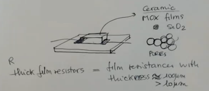
- ==They are THICK film resistances, so with a thickness, which is usually around micrometers==.
- ==When we speak about THIN film, instead, we think to films, which have a thickness of less than micrometers==.
- We have two electrodes, metal depositions, this may be thin, and on top, the active layer, the material which builds up the sensing device.
And usually, this film is not properly ceramic, because it’s made up of many different grains, so like powder, which stays together, but it has a lot of pores, so that gas can reach all the film in its whole thickness. - The thick film resistances is usually ceramic, it is inert, so it doesn’t interact with chemical compounds.
On the backside of the ceramic insulator (inert) substrate, usually you find a thin or thick film metal resistance, which acts as a heater (using the current we provide).
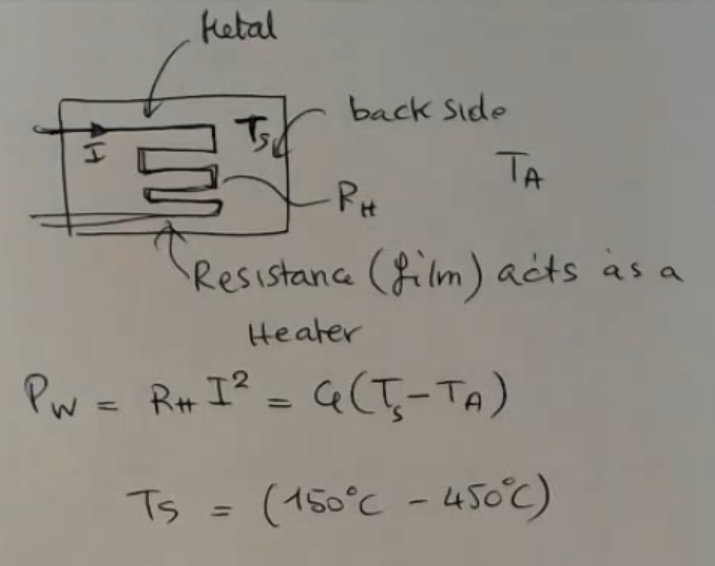
- : power of the ovareall device.
This power is something that depends on the size of the device. - : conductivity ().
- So we can use the temperature at relatively high temperature: in the range .
- The reason why it is necessary to bring this resistive sensor to a very high temperature is because the chemical reaction are faster at this higher temperature, which are needed to get the variation of the resistance.
Analysis of Two Grains of Material for Chemical Resisitve Sensors
The principle of operation for this sensor here is based on absorption.
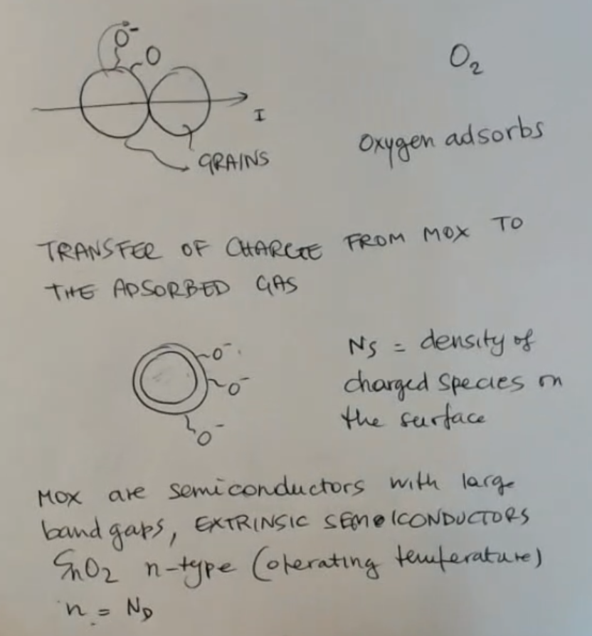
- We take only two grains from the thick film, the current has to pass through these two grains.
- On the surface of these grains here, the gas, which I want to sense, (let’s consider oxygen for instance) is absorbed.
- After being absorbed on the surface, there is a transfer of charge from the sensor (from the metal oxide) to the gas, and vice versa.
So for instance, oxygen tends to take an electron from the metal oxide, and it traps this electron, this negative charge, on the surface. - Now I have a charged species on the surface, with a certain density, which I call .
- In these metal oxide semiconductors, there are defects which are naturally present which acts as dopants.
⇒ ==So at these temperature these intrinsic semiconductors behave as extrinsic==.
So we have:
- what happens is that I have depleted the layer under the surface, so it mean that in this layer electrons are no longer present because they have been taken by the assortment compound, which is oxygen in this case.
⇒ ==We have a plus charge region under the surface, like in a diode==.
So obviously you have a minus charged layer, a positive charged layer, so you have an electrical field, and associated with this electrical field, you have a voltage barrier, which is like this:
- When you place two grains together and you want the current to flow through, at the surface of each grain there is the potential barrier.
⇒ So only the electrons which have enough energy to overcome this barrier can pass through to the next grain, and so contribute to the overall current in the film. - This is like a diode, and for this reason at the end, we can find the conductivity of the film, where:
- : height of the potential barrier between each grain of the substrate.
- : is the density of the absorbed and charged chemical compound.
- : is the temperature of the sensor.
- : is the density of dollars.
- : the constant of Boltzmann.
- : the electric permittivity.
Conclusions
Taken the conductivity formula:
- We see that the temperature of the sensor () has to be kept very, very constant, otherwise you have a reaction due to temperature which is of the same intensity as the reaction due to chemical compound concentration.
==The Selectivity of these devices is decided by the chemistry, some materials tend to absorb some gases, others instead other gases==. So by selecting this specific type of material or the dopants put into the material, you can change which kind of gas is absorbed.
Also, ==these are sensors which are not so reproducible==.
The processes which happen at the surface are quite not so known.
The final equation gives only an approximation of what really happens, and it can be very different on the basis of different material and different microstructure of the field.
⇒ Read carefully the data-sheet.
==One of the most important influence factor is the humidity which is the water vapor, always present in the environment. And also the change of temperature may really change the behavior of the sensor==.
~Ex.: Data Sheet of a Hydrogen Gas Sensor
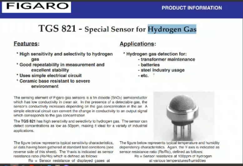
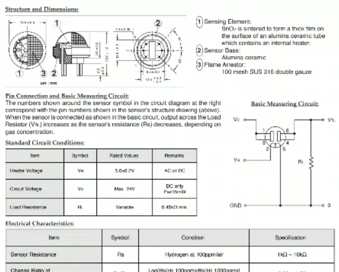
- This sensor is specifically for hydrogen gas and it’s meant for detection.
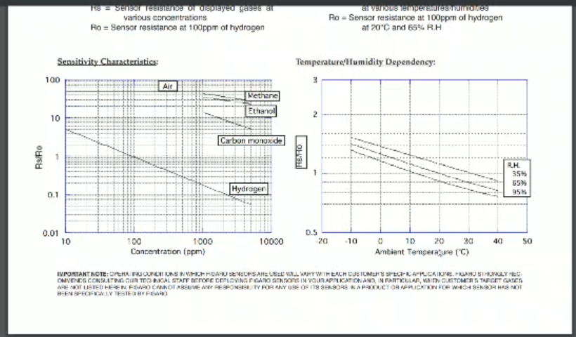
- ==And you see that in any case the sensitivity to hydrogen is very high but you have sensitivity also to other gases==.
- The response of the sensor is given as a log-log plot.
- As you can see, we have almost three decades of response variation.
So a large sensitivity for this kind of concentration range. - And also humidity you see has a deep impact on the behavior as I have told you of the sensor.
- ==These are Low Cost Devices==.
- ==They have many limitations (Temperature, Humidity, Selectivity)==.
- ==But at least they have good Sensitivity==.