List of things to memorize:
SaM - Resistive Sensors
Link to original
- SaM - Potentiometer
- SaM - Metal Strain Gauge • Passive Strain Sensor
- SaM - RTD Sensor
- SaM - Thermistor
- SaM - Thermocouples
- SaM - Photoresistance
- SaM - Magneto Resitances
- SaM - Chemical Resistive Sensor
- Terminology:
- : resistance.
- : displacement.
- : resistivity.
- : surface.
SaM - Metal Strain Gauge • Passive Strain Sensor:
- Principle of operation & Strucutre:
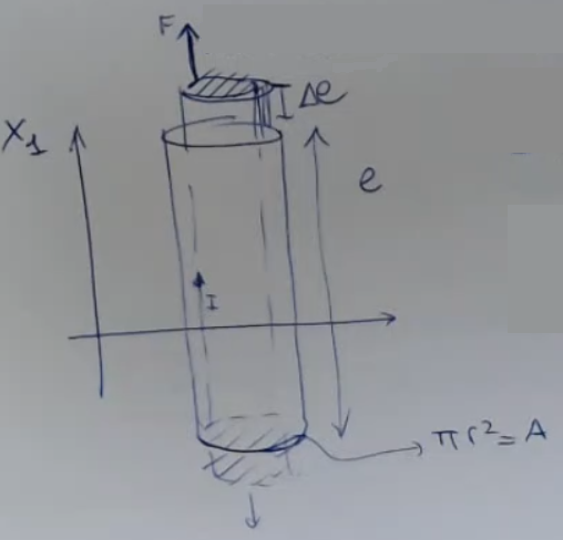
- Formula:
- G (Gauge) Factor:
- Considering the Transverse Sensitivity:
- Considering the Temperature Effect:Where:
- Real World Quantities:
- ⇒ variation of resisitance is really small (bad).
- .
- .
- ⇒ low TCR (good).
- Terminology:
- : gauge factor.
- : coefficient of piezoresisitivity.
- : Poisson modulus.
- or : parallel strain.
- : perpendicular strain.
- : transverse gauge factor.
- or : the TCR.
- : thermal exampansion.
- : thermal exampsion coefficients of the substrate.
- : thermal exampsion coefficients of the metal grid.
- : temperature.
- : temperature variation.
See Also
SaM - Photoresistance
- Workings of a Photoresistance:
- To use the “photoelectric effect”, we need a semiconductor with energy gap less then the energy of a photon .
- When a photon hits the material, it is able to free one electron from the valence band and promote it into the conduction band .
- So given a certain wavelength we will obatin a response in the form of more free carriers, so more conduction, ==⇒ less resistance==
- Energy of the photon:
- Minimum frequency:
- Maximum wavelenght:
- Conductance of a semiconductor:
- Total resistance of a photoresistance:
- This is more like a detector then a real sensor.
- Real World Measures:
- Visible light has a wavelength:
And a corresponding energy: - Cadmium sulfide semiconductor has an
- : lead sulfide, (used in Infra-Red Cameras).
- : lead selenide, (used in Infra-Red Cameras).
- : exponent for the photoresistance formula, is in the range
- For a photoresistance we have usually this ratio:
- Photoresistances are slow devices:
- Visible light has a wavelength:
- Terminology
- : energy gap.
- : wavelength.
- : frequency.
- : speed of light.
- : Planck’s constant.
- : conductance.
- charge of the electron.
- : ???
- : illuminance is measured in lux (measure unit)
- cd : candela (measure unit).
- sr : steradian (measure unit).
- : rise time.
SaM - Geometrical Magneto Resistance
- Current density equation:Can be rewritten as:Where:
- Geometrical magneto resistance formula:
- Terminology:
- : current density vector,
- : density of carriers.
- : charge of an electron or of a hole
- : velocity of carriers.
- : conductivity of the material.
- : electric field vector.
- : mobility of carriers.
- : magnetic field density.
Link to original
SaM - Types of Magneto Resistances
Given a certain magnetic field intensity a magneto-resistive material will change its resisitivity.
- An OMR (Ordany Mangeto Resitive) material can change its reisitivity up to a .
- There are also other types of mangeto resistances, these are all due to “quantistic effects”:
- GMR (Giant Magneto Resitance)
- CMR (Colossal Magneto Resitance)
- TMR (Tunnel effect Magneto Resitance)
Link to original
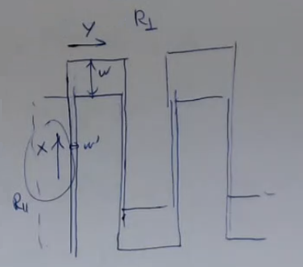
SaM - Anisotropic Magneto Resistance (AMR) • Easy Axis • Barber Pole • Honeywell
- Materials that present AMR, like: Ni, Fe and Permalloy (Fe + Ni).
- AMR Formula:
- Easy axis , an axis taken in the same direction of
- If we have that than we can approximate:
- AMR Formula using the approximation:
- Total resisitance value:Where:
- Graph of given :
- At the sensor behaves linearly.
- Rotate the current with a barber pole:
- Simplified resistance formula for a barber pole:
- Honeywell or resistive bridge:
- Formula of the Honeywell:We can also calculate the relative sensitivity as: Remember that:
- Magnetic angle sensors formula:Where:
- or , refers to a honeywell bridge sensing along the axis.
- or refers to the honeywell bridge sensing along the axis.
- Terminology
- is the resisitivity when .
- is the resisitivity when .
- is the angle formed by and , where:
- : current density vector,
- is the total magnetization vector, accounting for the external magnetic filed , and for the magnetization of the material ,
- is the saturation field, it is a property of the material.
- : resisitvity.
- is the output.
- is the relative sensitivity, and for this structures it is usually .
- is the input voltage.
- is the external magnetic field density.
Link to original
/../../Notes--and--Images/Pasted-image-20230718200022.png)
/../../Notes--and--Images/Pasted-image-20230718200035---Copia-1.png)
/../../Notes--and--Images/Pasted-image-20230718200128-1.png)
SaM - Chemical Resistive Sensor
- Structure:
- Thick film ceramic resistances (an inert material).
- Two metal electrodes.
- An active layer (a pourus material, ~ex.: like a mox film).
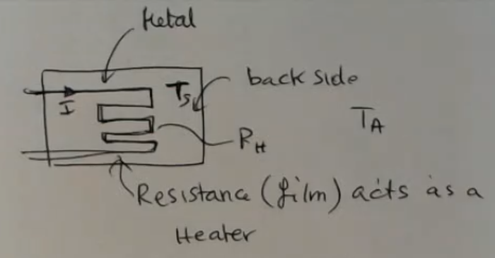
- Thick film metal resisitance on the backside (a heater).
- Topside view:
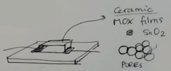
- Backside view:
- Principle of Operation:
- This sensor is based on absorption.
Meaning the active layer is a granular material that trap or absorb, different compounds. - After being absorbed on the active layer, there is a transfer of charge from it (from the metal oxide - mox film) to the gas, and vice versa.
~Ex.: oxygen tends to take an electron from the metal oxide, and it traps this electron, this negative charge, on the surface. - We have a plus charge region under the surface, like in a diode.
- When many of these “diode-granes” are put togheter they resist the flow of current, so we have increased the reisitance of the sensor.
- This sensor is based on absorption.
- Sensitivity:
- Sensitivity to a different compound:⇒ ==Chemical Resistive Sensor are non-selective devices==.
- Power used to opertate this device:
- Conductivity of the device:
- Other things to memorize:
- Chemical Resistive Sensor are non-selective devices.
- This is more like a detector than a real sensor.
- Why we need a heater.
- Why the temperature of the sensor should be kept constant.
- These sensors are not so reproducible.
- The humidity (water vapor), always present in the environment, can influence the resitance value.
- Real World Measures:
- Thick film : ( : thickness).
- Thin film : ( : thickness).
- .
- Terminology:
- inert : meaning it doesn’t interact with chemical compounds.
- : specific compund the sensor is designed for.
- : non-spefic compund the sensor is NOT designed for .
- : power of the overall device.
- : conductance.
- : height of the potential barrier between each grain of the substrate.
- : density of the absorbed and charged chemical compound.
- : temperature of the sensor.
- : density of donors.
- : Boltzmann’s constant.
- : electric permittivity
- : electric permittivity of the void
- : relative electric permittivity